Preparation method and application of grain boundary layer ceramic material and grain boundary layer ceramic substrate

A technology of ceramic substrates and ceramic materials, which is applied in the field of grain boundary layer ceramic materials, can solve problems affecting the repeatability and consistency of electrical properties of ceramic substrates in grain boundary layers, and achieve high repeatability and consistency of electrical properties. The effect of reducing the amount and increasing the degree of penetration

Active Publication Date: 2020-11-10
GUANGZHOU AURORA TECHNOLOGIES CO LTD +1
View PDF17 Cites 8 Cited by
  • Summary
  • Abstract
  • Description
  • Claims
  • Application Information

AI Technical Summary

Problems solved by technology

[0004] At present, there are still some problems in the electrical properties and controllability of grain boundary layer ceramic materials, which in turn affect the electrical performance repeatability and consistency of grain boundary layer ceramic substrates.

Method used


Image

  • Preparation method and application of grain boundary layer ceramic material and grain boundary layer ceramic substrate
  • Preparation method and application of grain boundary layer ceramic material and grain boundary layer ceramic substrate
  • Preparation method and application of grain boundary layer ceramic material and grain boundary layer ceramic substrate

Examples


preparation example Construction

[0036] The invention provides a preparation method of a grain boundary layer ceramic substrate, comprising the following steps:

[0037] Mixing the grain boundary layer ceramic material, the adhesive and the organic solvent described in the above technical solution, and molding to obtain the diaphragm;

[0038] The diaphragm is degummed and reduced fired in one step to obtain a semiconducting grain ceramic substrate;

[0039] coating the oxidant dispersion on the surface of the semiconducting grain ceramic substrate to obtain a semiconducting grain ceramic substrate with an oxide dielectric film attached;

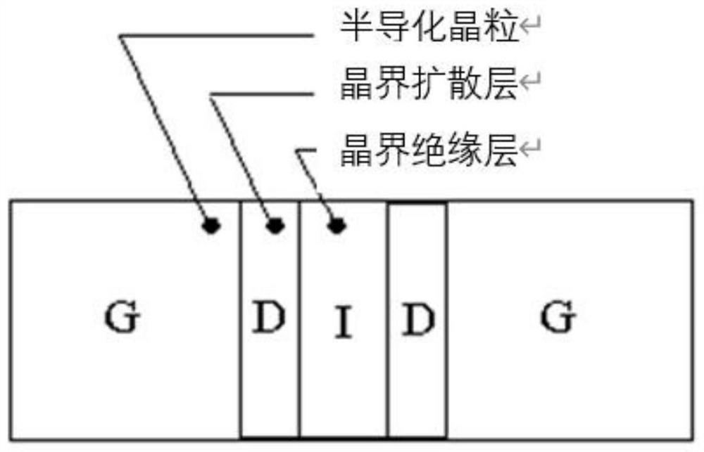
[0040] In a pure oxygen atmosphere, the semiconducting grain ceramic substrate attached with the oxide dielectric film is oxidized and heat-treated to form a grain boundary insulating layer to obtain a grain boundary layer ceramic substrate.

[0041] In the present invention, the grain boundary layer ceramic material described in the above technical solution, adhesive and ...

Embodiment 1

[0058] Grain boundary layer ceramic material preparation: 98.95 parts by weight of SrTiO 3 , 0.38 parts by weight of Nb 2 o 3 , 0.36 parts by weight of SiO 2 and 0.32 parts by weight of Sm 2 o 3 The mixed material is ball milled, dried and sieved in turn to obtain ceramic powder with an average particle size of D 50 0.62μm;

[0059] 57.39 parts of the grain boundary layer ceramic material, 14.51 parts of xylene, 14.51 parts of absolute ethanol, 3.70 parts of PVB B-980 and 3.09 parts of BBP S-1609 were mixed, and formed by casting to obtain a diaphragm (with a thickness of 0.20 mm), cut the diaphragm according to the size required by the product;

[0060] Put the diaphragm into a bowl in the form of a single-piece compartment, put it into an atmosphere furnace, and pass compressed air into the temperature curve of 100-900°C (the heating rate is 0.6°C / min) for debinding, after the debinding is completed After insulated at 900°C for 1 hour, a mixed atmosphere of hydrogen a...
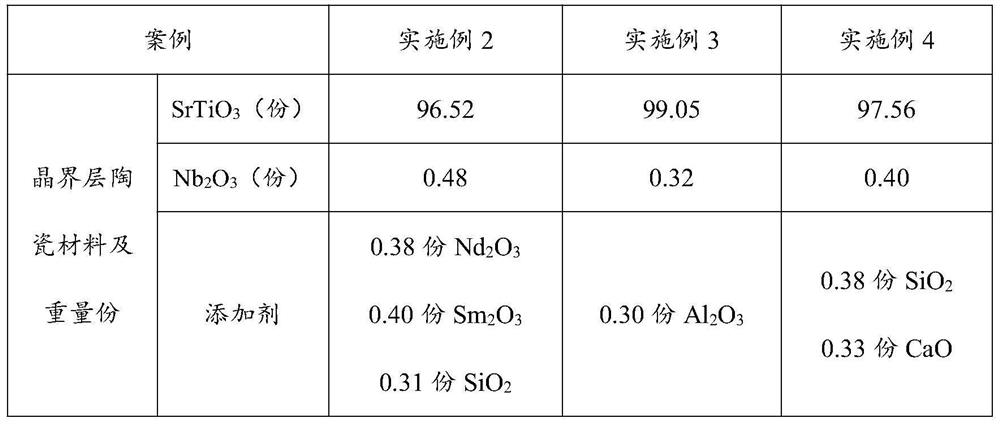
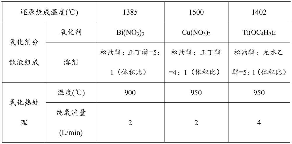
Embodiment 2~4

[0065] According to the preparation method of Example 1, adopt the grain boundary layer ceramic material ratio, firing temperature, electrophoresis process parameters and oxidation process as shown in the following table 1 to prepare the grain boundary layer ceramic substrate, the process and reagents not listed in the table Consumption is all identical with embodiment 1.

[0066] The parameter of table 1 embodiment 2~4

[0067]

[0068]

[0069] The grain boundary layer ceramic substrates prepared in the above-mentioned Examples 1 to 4 were cut into 2×2mm through sputtering metal electrodes. 2 Die, measure the electrical properties of the dice. According to K=11.3Ct / S (K is the dielectric constant of calculation, C is the capacitance measured, t is the thickness of the substrate, S is the chip area) calculate the grain boundary layer ceramic substrate sample that embodiment 1~4 prepares the dielectric constant. Take 10 samples from the four corners and the middle of ...


PUM

PropertyMeasurementUnit
particle sizeaaaaaaaaaa
thicknessaaaaaaaaaa
thicknessaaaaaaaaaa

Abstract

The invention provides a preparation method and application of a grain boundary layer ceramic material and a grain boundary layer ceramic substrate, and belongs to the technical field of chip capacitors. The grain boundary layer ceramic material provided by the invention is prepared from the following preparation raw materials in parts by mass: 95.35 to 99.30 parts of SrTiO3, 0.30 to 0.55 part ofNb2O3 and 0.30 to 5.00 part of a modification additive comprising one or more of BaCO3, Nd2O3, CaO, Sm2O3, Al2O3 and SiO2. The grain boundary layer ceramic material has excellent electrical propertiesand controllability, and a grain boundary layer ceramic substrate prepared from the grain boundary layer ceramic material has excellent repeatability and consistency.

Description

technical field [0001] The invention relates to the technical field of chip capacitors, in particular to a grain boundary layer ceramic material, a preparation method of a grain boundary layer ceramic substrate and an application thereof. Background technique [0002] In the defense industry technology, chip capacitors are more and more widely used. Since the chip capacitor adopts a single-layer structure, compared with the MLCC multilayer ceramic capacitor, there is no current loop between the dielectric layers, so it has very low ESR (equivalent series resistance) and ESL (equivalent series inductance), especially suitable for High-frequency applications such as radar, navigation, and satellite communications. [0003] Grain boundary layer ceramic material due to the use of SrTiO 3 At the same time, the technology of AB position precise chemical doping is adopted, which has the characteristics of high dielectric constant, stable temperature characteristics and superior m...

Claims


Application Information

Patent Timeline
Patent Type & Authority Applications(China)
IPC IPC(8): C04B35/47C04B35/622C04B41/87
CPCC04B35/47C04B35/622C04B41/009C04B41/5027C04B41/5041C04B41/5074C04B41/87C04B2235/3208C04B2235/3215C04B2235/3217C04B2235/3224C04B2235/3251C04B2235/3418C04B2235/5445C04B2235/602C04B2235/6025C04B2235/656C04B2235/6562C04B2235/6567C04B2235/6582C04B2235/6583C04B41/4535C04B41/0072
Inventor 冯毅龙吕明卢振亚陈炜豪
Owner GUANGZHOU AURORA TECHNOLOGIES CO LTD
Why Eureka
Try Eureka