A Method of Controlling Pn Junction Defect Energy Level Based on Electron Irradiation

A technology of defect energy level and electron irradiation, which is applied in the manufacture of circuits, electrical components, semiconductors/solid-state devices, etc., and can solve problems such as performance degradation

Active Publication Date: 2020-05-08
BEIJING UNIV OF TECH
View PDF3 Cites 0 Cited by
  • Summary
  • Abstract
  • Description
  • Claims
  • Application Information

AI Technical Summary

Problems solved by technology

But the key that actually affects the performance of the irradiated device is the position and concentration of the defect level introduced into the PN junction. The closer the position of the defect level to the center of the forbidden band, the higher the defect concentration, the more obvious the recombination effect, and the shorter the minority carrier lifetime of the device. Low, but other performance degradation is more serious

Method used


Image

  • A Method of Controlling Pn Junction Defect Energy Level Based on Electron Irradiation
  • A Method of Controlling Pn Junction Defect Energy Level Based on Electron Irradiation
  • A Method of Controlling Pn Junction Defect Energy Level Based on Electron Irradiation

Examples


Embodiment 1

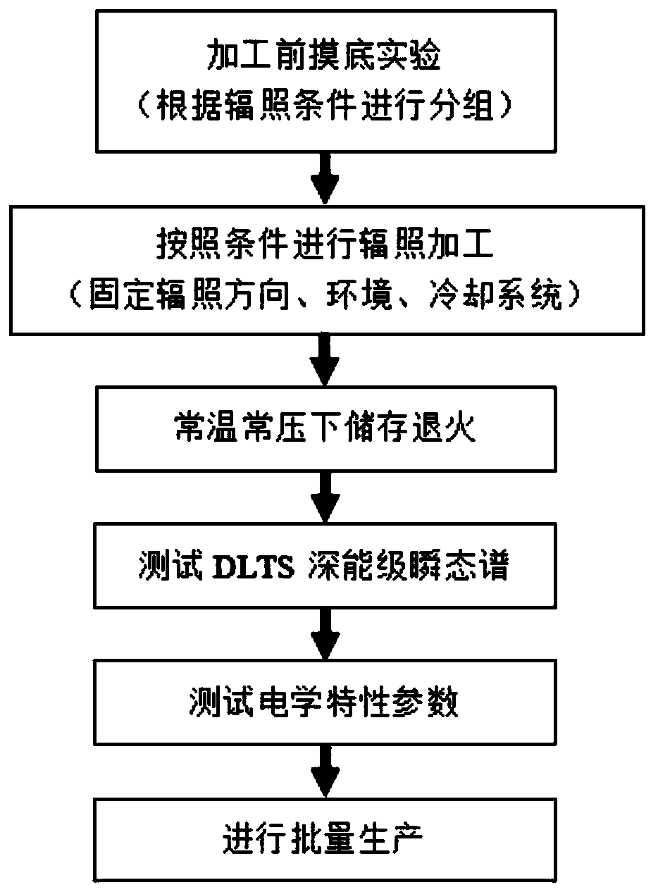
[0020] Embodiment 1 The method of the present invention for controlling the energy level of PN junction defects based on electron irradiation includes the following steps:

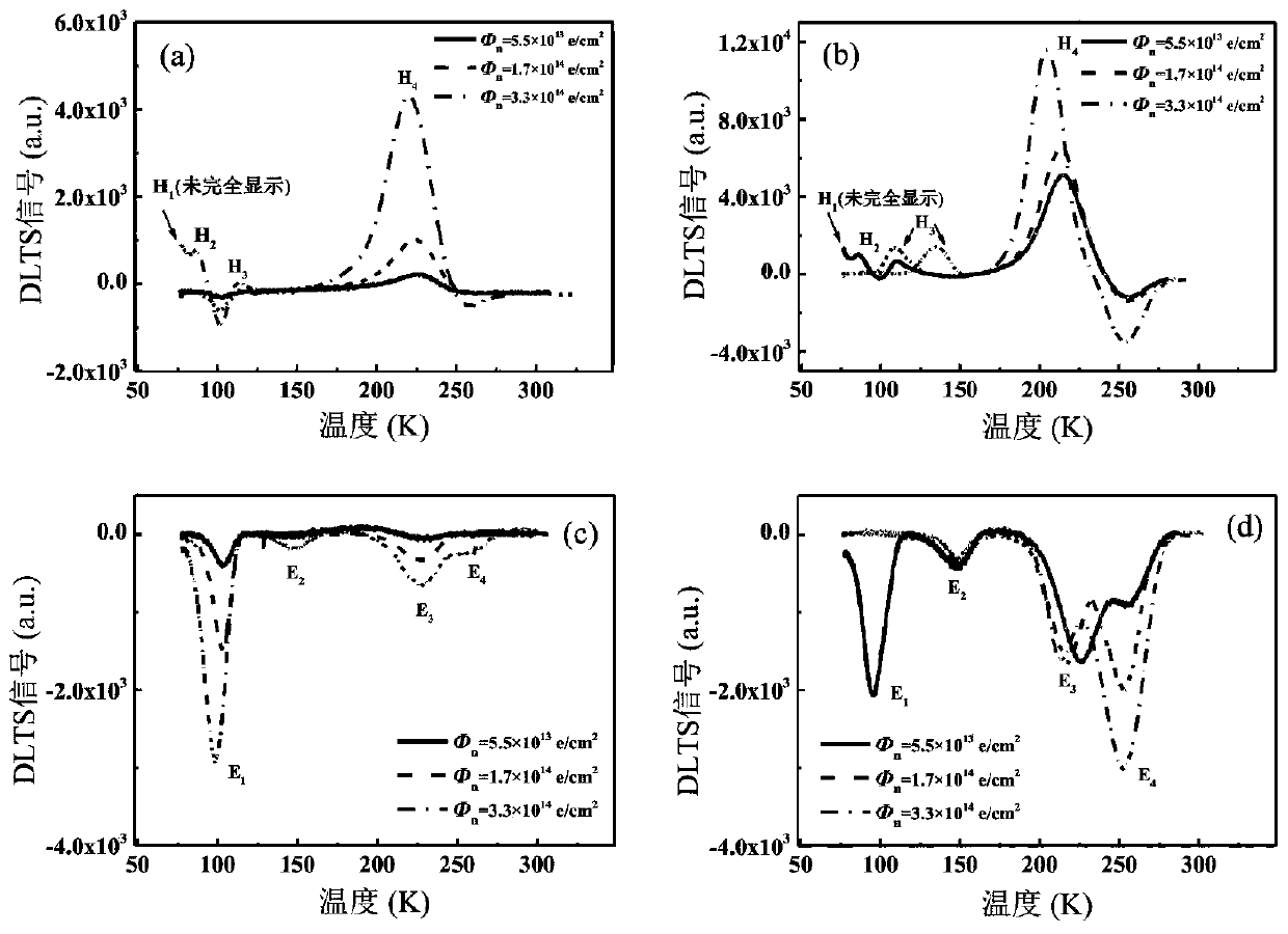
[0021] (1) Group the 1N4007 n-Si rectifier diodes that require performance optimization before irradiation. According to two kinds of irradiation energy 2.0, 5.0MeV and three kinds of irradiation fluence 5.5×10 13 , 1.7×10 14 , 3.3×10 14 e / cm -2 (I.e. irradiation time 30, 90, 180s) The conditions are divided into 6 groups, and there is a non-irradiated comparison group, a total of 7 groups, each group contains 3 devices.

[0022] (2) Use 2.0 and 5.0MeV linear electron accelerators to irradiate the device under test, respectively, the irradiation fluence is 5.5×10 13 , 1.7×10 14 , 3.3×10 14 e / cm -2 , That is, the irradiation time is 30, 90, 180s.

[0023] (3) The electron beam intensity of the electron accelerator used is 0.1mA, and the current is unstable <±2%, unevenness <±5%.

[0024] (4) The irradiation environ...


PUM


Abstract

The invention discloses a method for controlling a defect level of a PN junction based on electron irradiation. The method comprises the steps of (1) performing a baseline experiment prior to primary processing and grouping devices according to an irradiation condition; (2) performing irradiation processing on the devices according to the irradiation condition and fixing an irradiation direction, an irradiation environment and a cooling system; (3) storing the devices at normal temperature and pressure to achieve stable properties; (4) testing DLTS (Deep Level Transient Spectroscopy) and determining position, concentration and capture cross section parameters of the defect level; (5) testing electrical characteristic parameters which include a forward characteristic, a reverse characteristic and a switching characteristic; and (6) performing massive processing and production. The method can control the position and concentration parameters of the defect level by changing the electron irradiation condition, is good in repeatability, can achieve the massive processing after early testing, and can realize an objective of oriented optimization for various properties of the devices according to a production demand.

Description

Technical field [0001] This technology relates to the field of radiation modification. It is mainly used to control defect energy level parameters in PN junction using electron irradiation. Background technique [0002] As the operating frequency of power switching devices continues to increase, the requirements for the switching speed and comprehensive performance of the fast recovery diodes connected in parallel are also increasing. Electronic radiation modification technology has replaced gold and platinum doping technology as one of the commonly used device performance optimization technologies due to its advantages of good consistency, simple process, and low cost. The main goal of optimizing the performance of the diode is to use different life control technologies. By introducing the defect energy level as a recombination center in the band gap, the minority carrier life can be reduced and the switching speed should be increased. At the same time, it is necessary to ensur...

Claims


Application Information

Patent Timeline
Patent Type & Authority Patents(China)
IPC IPC(8): H01L21/268H01L21/66
CPCH01L21/268H01L22/20
Inventor 郭春生王若旻冯士维
Owner BEIJING UNIV OF TECH
Why Eureka
Try Eureka