Component for semiconductor package and manufacturing method of component for semiconductor package

a manufacturing method and semiconductor technology, applied in resist details, non-metallic protective coating applications, patterning and lithography, etc., can solve the problems of difficult to form fine patterns, problems such as and achieve the effect of reducing the reliability of the solder resist layer formed

Inactive Publication Date: 2009-05-14
SHINKO ELECTRIC IND CO LTD
View PDF6 Cites 12 Cited by
  • Summary
  • Abstract
  • Description
  • Claims
  • Application Information

AI Technical Summary

Benefits of technology

[0009]Exemplary embodiments of the present invention provide a component for semiconductor package comprising a protective insulating layer of a high-accuracy fine pattern which cannot be formed in a printing method and is manufactured using a protective insulating material (in other words, a nonphotosensitive protective insulating material) without including a photosensitive expression substance which may decrease reliability of a solder resist layer formed, and a manufacturing method of such a component for semiconductor package.

Problems solved by technology

As a result of that, reliability of the solder resist layer formed may become a problem in the case of the patterning method using the photosensitive solder resist material.
With increasing miniaturization of an electronic component including a semiconductor chip, a printed pattern also becomes finer and it becomes difficult to form a fine pattern with high accuracy in the printing method using the mask.

Method used


Image

  • Component for semiconductor package and manufacturing method of component for semiconductor package
  • Component for semiconductor package and manufacturing method of component for semiconductor package
  • Component for semiconductor package and manufacturing method of component for semiconductor package

Examples


Embodiment Construction

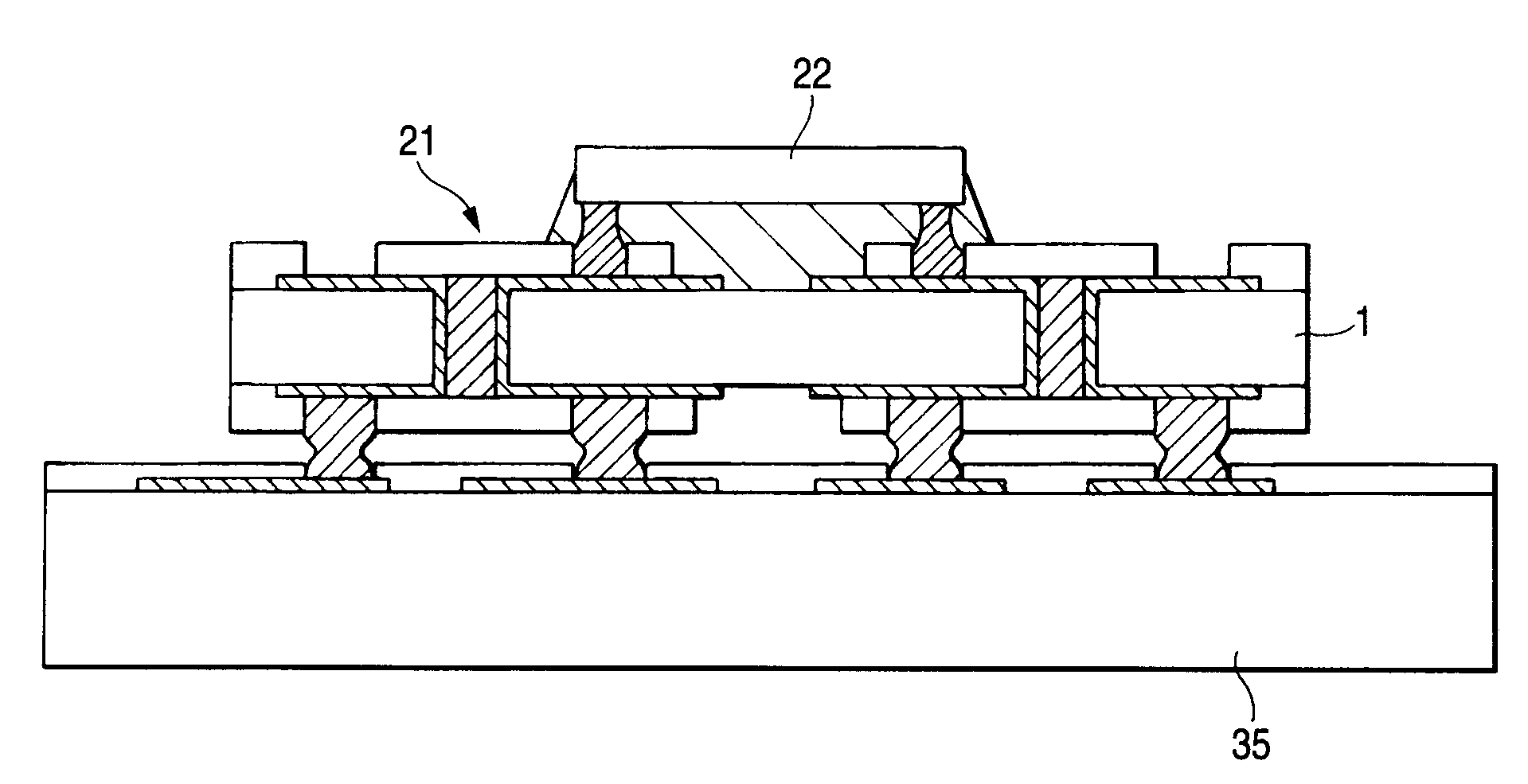
[0025]A component for semiconductor package manufactured by a method of the invention is a component used for fabricating a semiconductor package used for installing a semiconductor chip and mounting the semiconductor chip on a mounting substrate etc., and a wiring substrate (generally, an organic substrate in which a predetermined number of wiring layers are formed) or a lead frame are typical.

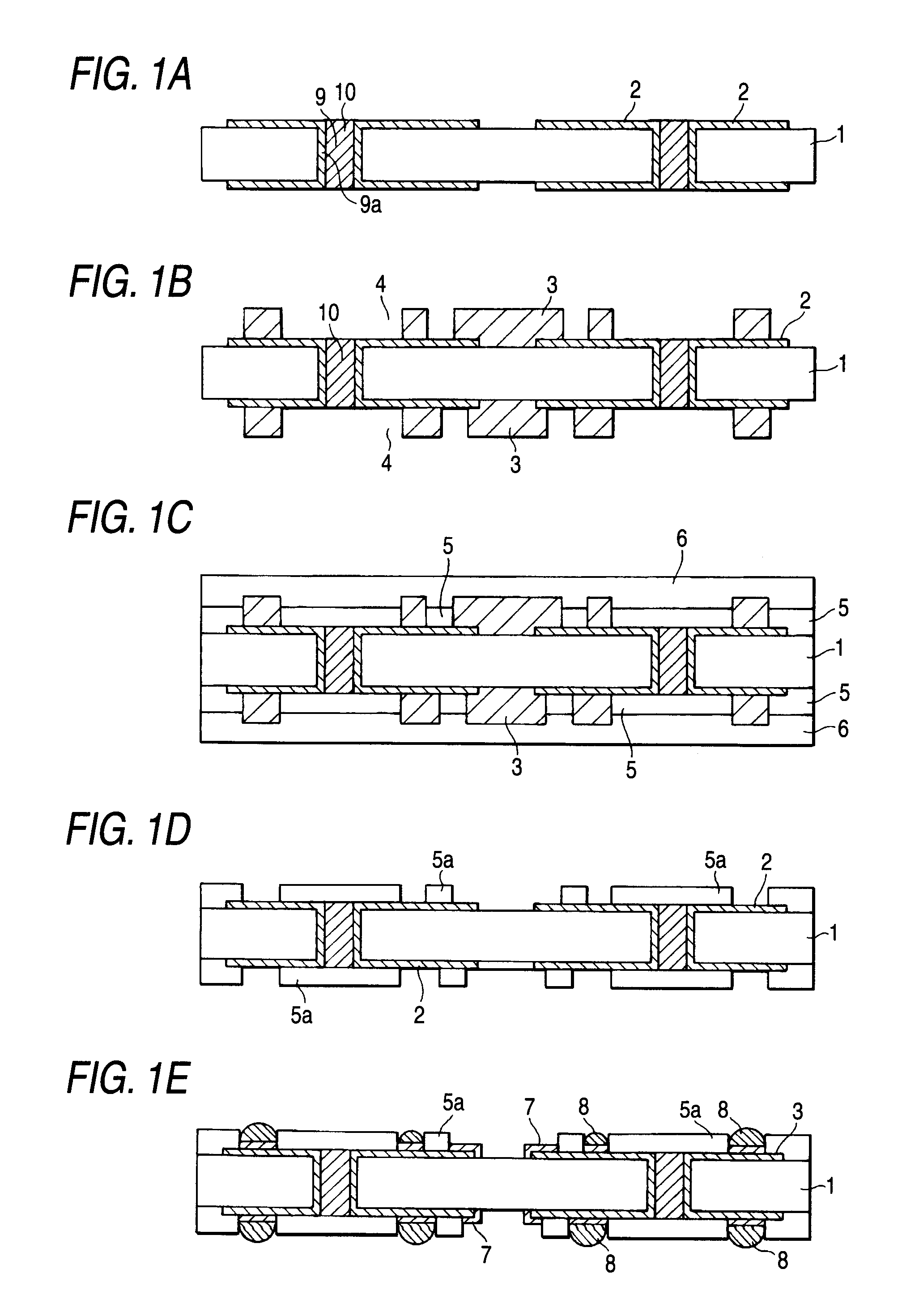
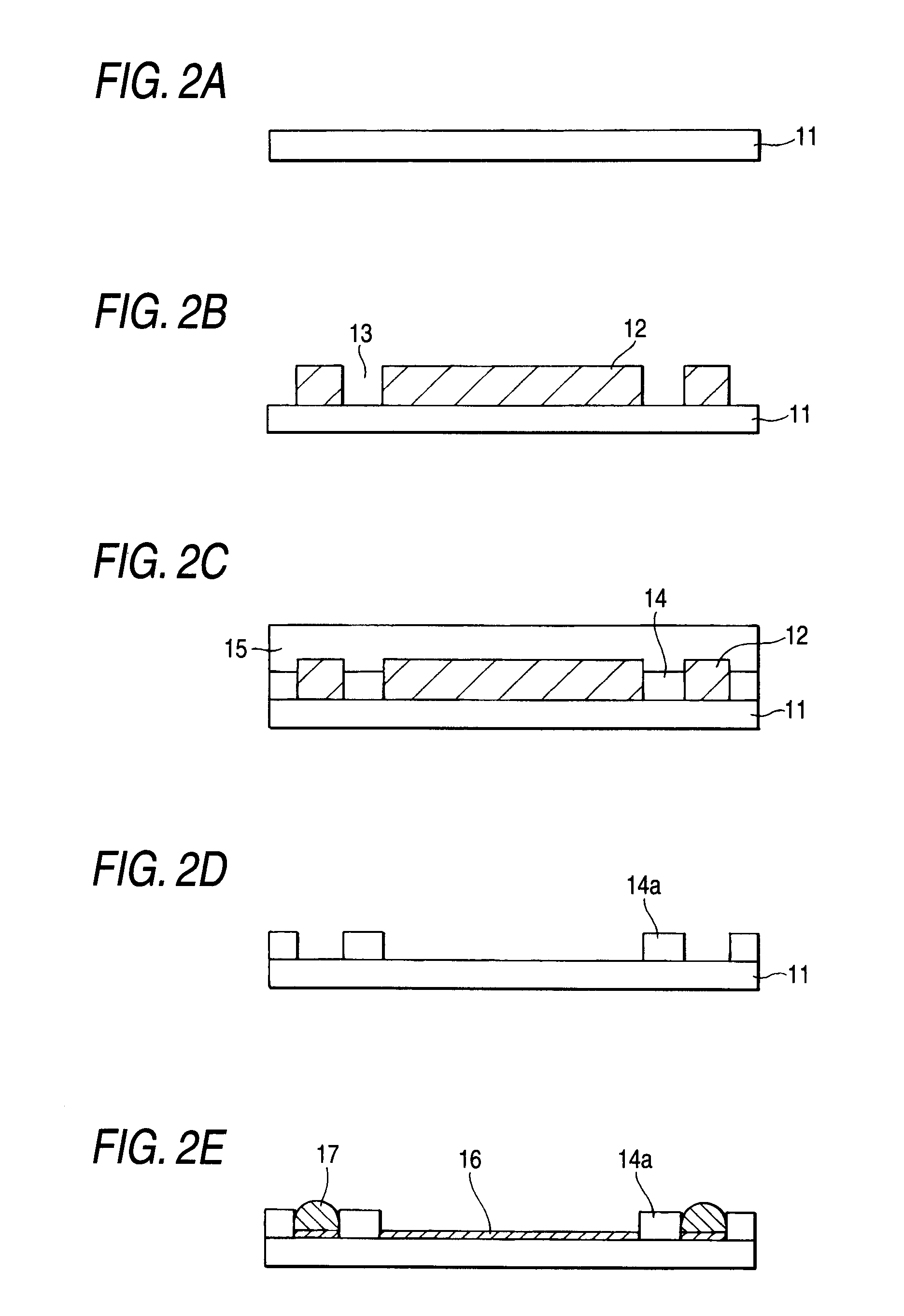
[0026]A “component body” in a manufacturing method of the component for semiconductor package of the invention refers to a semi-finished product before a protective insulating film for exposing a part of the wiring layer is formed, the semi-finished product having a wiring layer formed by a conductive material on at least one surface. A typical example of such a component body is a wiring substrate before a protective insulating layer is formed on at least one side, the wiring substrate having a wiring layer on at least one surface (may have one or more wiring layers in the inside or may have...


PUM

PropertyMeasurementUnit
conductiveaaaaaaaaaa
photosensitiveaaaaaaaaaa
photosensitivityaaaaaaaaaa

Abstract

A component for semiconductor package which has a protective insulating layer on at least one surface of a component body and exposes a conductive material of the component body to an opening part of the protective insulating layer is manufactured by a method including the steps of (a) forming a mask on at least one surface of the component body, (b) forming the protective insulating layer by filling an opening part of the mask with a protective insulating material by a molding method using a metal mold comprising a mold release film, and (c) removing the metal mold and removing the mask. A typical component is a lead frame or a substrate for semiconductor package.

Description

TECHNICAL FIELD[0001]The present disclosure relates to a component for semiconductor package and a manufacturing method of the component for semiconductor package. Particularly, the present disclosure relates to a component such as a lead frame for semiconductor package or a substrate for semiconductor package used in the case of mounting a semiconductor chip in a mounting substrate, and a manufacturing method of such a component.RELATED ART[0002]In the case of mounting a semiconductor chip, a component for installing the chip and mounting the chip in a mounting substrate is used. For example, a technique for installing a semiconductor chip in a mounting substrate using a semiconductor package fabricated by installing the semiconductor chip in a substrate for package is widely used.[0003]A related-art substrate for semiconductor package is generally fabricated as a wiring substrate in which multilayer wiring is formed in an organic core substrate by a build-up method. A semiconducto...

Claims


Application Information

Patent Timeline
Patent Type & Authority Applications(United States)
IPC IPC(8): H01L23/12H01L21/00
CPCH01L21/4867H05K2203/0582H05K3/28H01L2224/16225H01L2224/32225H01L2224/48091H01L2224/48227H01L2224/73204H01L2224/73265H01L2924/15311H01L2924/00014H01L2924/00H01L23/02H01L23/04
Inventor OI, KIYOSHICHINO, TERUAKI
Owner SHINKO ELECTRIC IND CO LTD
Why Eureka
Try Eureka