High time-resolution ultrasensitive optical sensor using a planar waveguide leakage mode, and methods for making same

a planar waveguide leakage and ultra-sensitive technology, applied in the field of high-time-resolution ultra-sensitive optical detectors, can solve the problems of limited performance, hardly exceeding this value, and technological limitations

Inactive Publication Date: 2009-05-21
COMMISSARIAT A LENERGIE ATOMIQUE ET AUX ENERGIES ALTERNATIVES
View PDF3 Cites 17 Cited by
  • Summary
  • Abstract
  • Description
  • Claims
  • Application Information

AI Technical Summary

Problems solved by technology

SSPD potentially have all the qualities mentioned above and are good candidates to replace the present avalanche photodiodes and photomultiplicator tubes, the performance of which is limited, particularly in the infrared domain.
It can hardly exceed this value on account of the present technological limitations, associated with the electronic lithography that is used to form the serpentine structure.
Better overlap ratios may be envisaged with other techniques, but a structure in which the meanders are too close favours cross-talk and necessitates an increased length of superconducting material.
The only way of increasing it would be to increase the thickness of the NbN layer, but the ratio between the section of the hot spot and the section of the superconducting strip would decrease, since the width of this strip is limited to around 100 nm, and that would cause a collapse in the overall efficiency (see [Korneev 03]).
It would probably be difficult to do better, since the long length of the NbN track (150 μm to 200 μm when this track is unwound) h

Method used


Image

  • High time-resolution ultrasensitive optical sensor using a planar waveguide leakage mode, and methods for making same
  • High time-resolution ultrasensitive optical sensor using a planar waveguide leakage mode, and methods for making same
  • High time-resolution ultrasensitive optical sensor using a planar waveguide leakage mode, and methods for making same

Examples


Embodiment Construction

[0034]The present invention aims to resolve the problem of the design of a high time-resolution ultrasensitive optical detector, in particular a SSPD type detector, said detector having a detection efficiency clearly superior to those that are obtained in the prior art, this detector moreover being able to be produced by existing technological means.

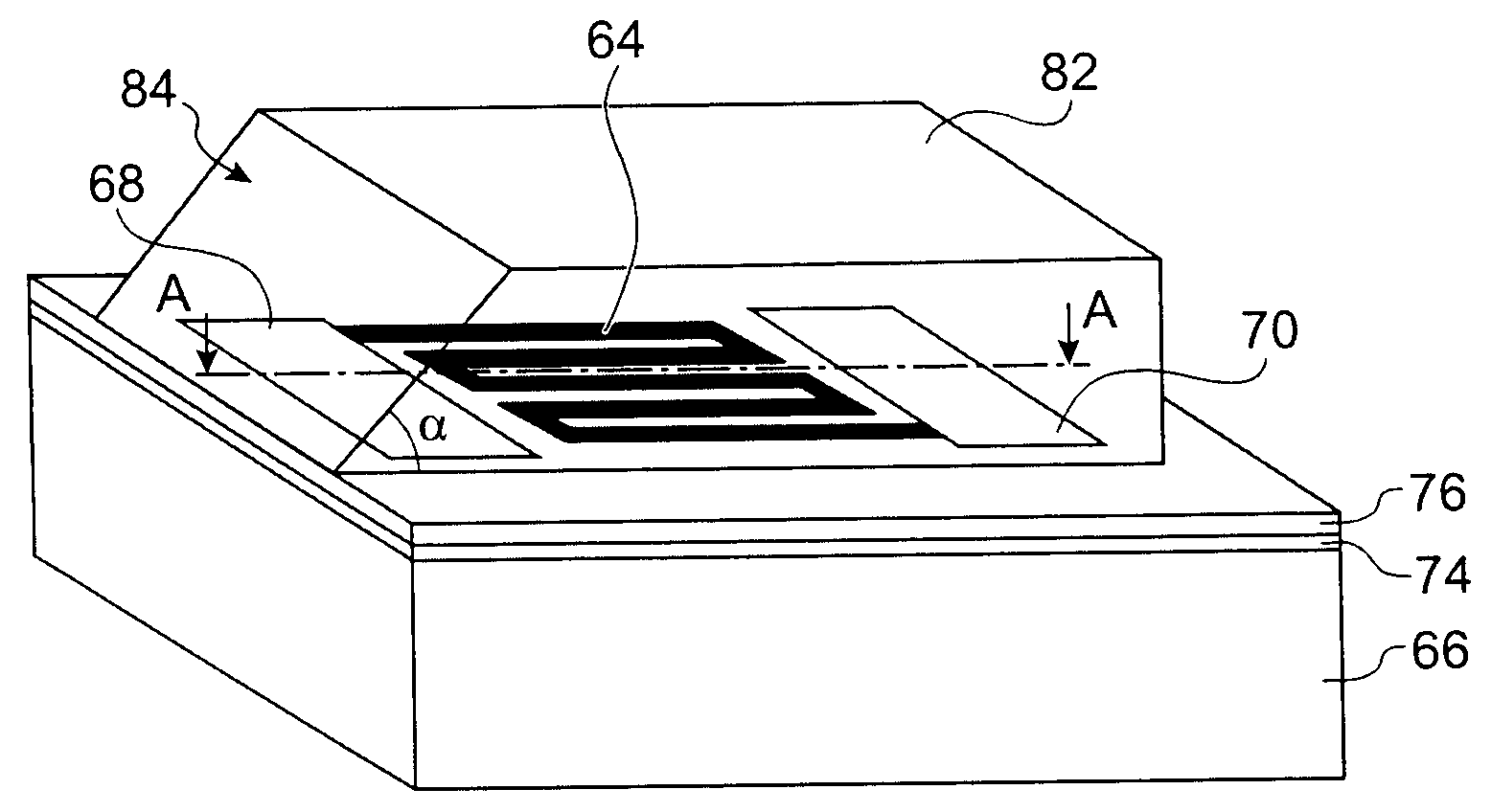
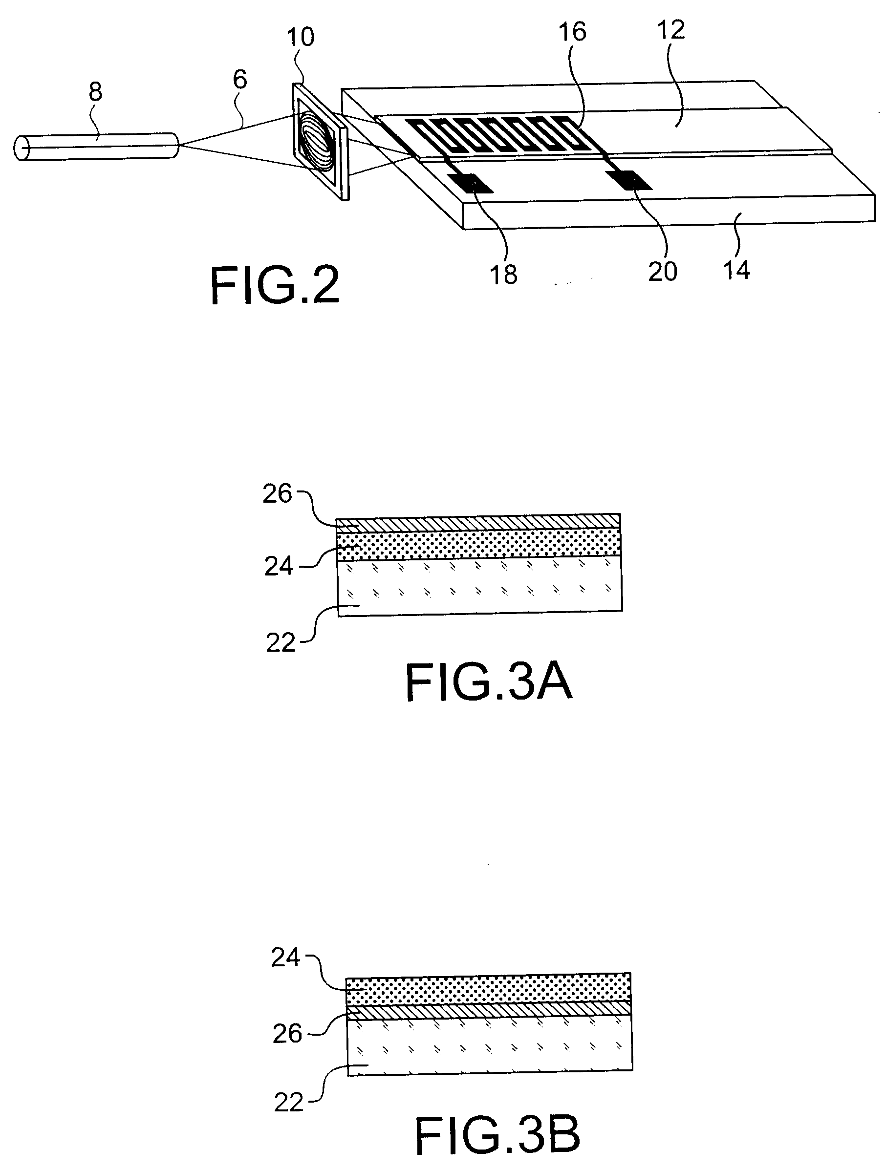
[0035]In a precise manner, the subject of the present invention is an optical detector, intended to detect at least one photon, this detector comprising a stacking with a dielectric substrate having a refractive index nS and, on this substrate:[0036]a detection element, provided to generate an electrical signal from the energy of the photon(s) received, and[0037]a first dielectric layer having a refractive index nH,

[0038]this detector being characterised in that it further comprises:[0039]a second dielectric layer, placed on the first dielectric layer and having a refractive index nB, nH being greater than nB and nS, the detection elemen...


PUM


Abstract

A high time-resolution ultrasensitive optical detector, using a planar waveguide leakage mode, and methods for making the detector. The detector includes a stacking with a dielectric substrate, a detection element, first and second dielectric layers, and a dielectric superstrate configured to send photon(s) into the light guide formed by the first layer. The thicknesses of the layers is chosen to enable a resonant coupling between the photon(s) and a leakage mode of the guide, the stacking having an absorption resonance linked to the leakage mode for a given polarization of the photon(s).

Description

TECHNICAL FIELD[0001]The present invention concerns a high time-resolution ultrasensitive optical detector and, in particular, a superconducting single photon detector, more simply known as SSPD.[0002]The detector that is the subject of the invention uses a planar waveguide leakage mode.[0003]The present invention further concerns methods for making said detector.[0004]It applies in particular to the detection and the localisation of operating defects of a semi-conductor integrated circuit, by detection of the emission of specific photons by malfunctioning transistors.[0005]It also applies to receiving and routing circuits for very high speed telecommunications, in particular to those that are intended for telecommunications satellites, on account of the very low heat dissipation of the detector that is the subject of the invention.[0006]The invention further applies to the coding and the detection of the quantum code key in a cryptographic system.[0007]It also applies to the manufa...

Claims


Application Information

Patent Timeline
IPC IPC(8): H01L39/00G01J5/00G01T1/24
CPCG01J1/02G01J1/0209G01J1/42G01J1/0407G01J1/0477G01J1/04
Inventor FREY, LAURENT
Owner COMMISSARIAT A LENERGIE ATOMIQUE ET AUX ENERGIES ALTERNATIVES
Why Eureka
Try Eureka