

Reference voltage generation circuit, ad converter, da converter, and image processor
- Summary
- Abstract
- Description
- Claims
- Application Information
AI Technical Summary
Benefits of technology
Problems solved by technology
Method used
Image

Examples
first embodiment
Modified Example of First Embodiment
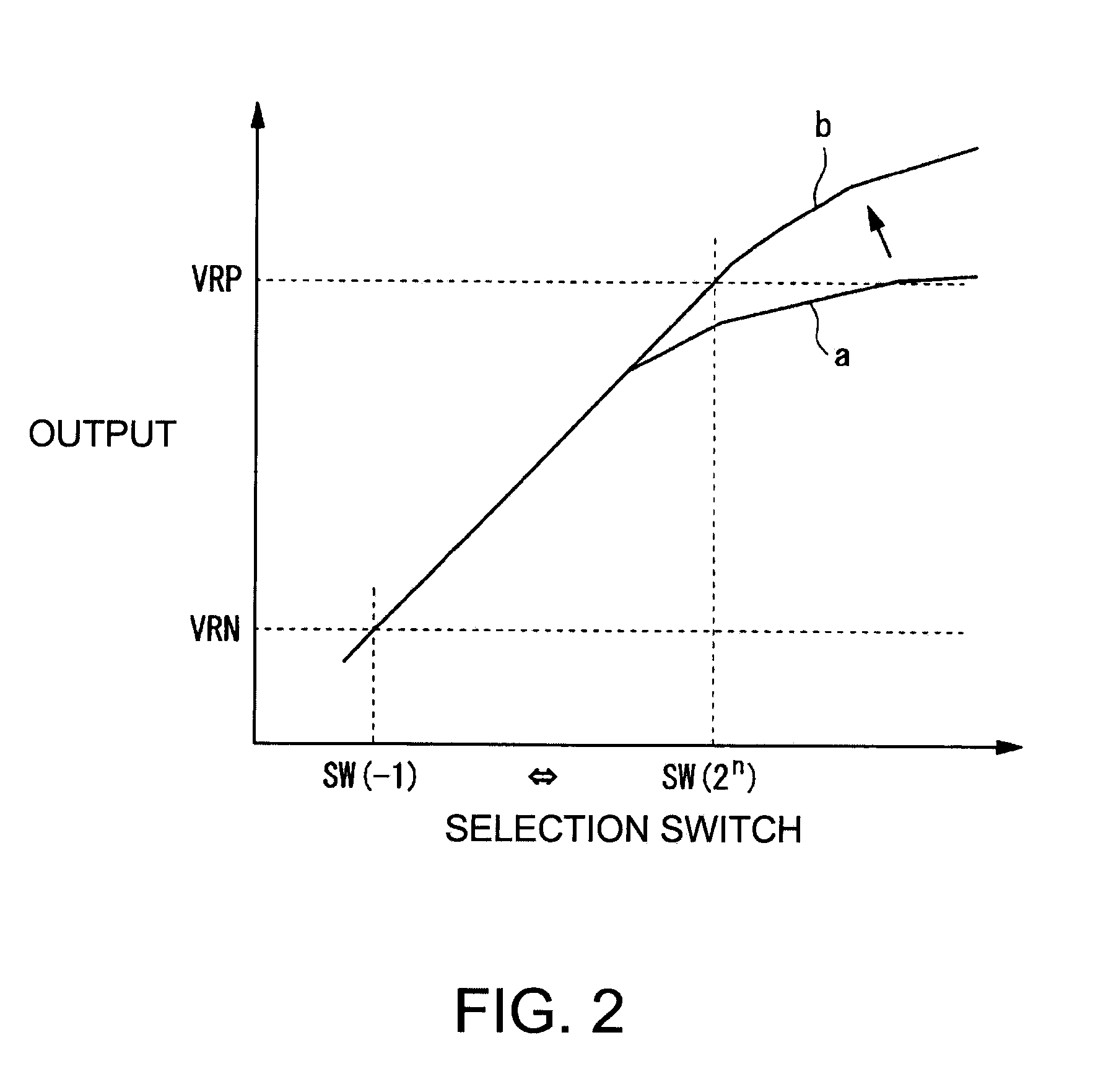
[0058]The modified example is so constituted that the NMOS transistors forming the analogue switches of the first embodiment in FIG. 1 are replaced with the PMOS transistors. In the case of the PMOS transistors, the sizes (W / L) of the transistors are increased stepwise from the analogue switch for selecting the highest reference voltage to the analogue switch for selecting the lowest reference voltage.
[0059]Accordingly, in a case where the sizes are varied stepwise, the size of the analogue switch for selecting the highest reference voltage is made minimum, and the size of the analogue switch for selecting the lowest reference voltage is made maximum.
[0060]By satisfying the above concept, the sizes of the transistors can be determined as in the case of the NMOS transistors. By using the modified example in the above described structure, it is possible to achieve the active effect the same as that of the first embodiment.
second embodiment
of Reference Voltage Generation Circuit
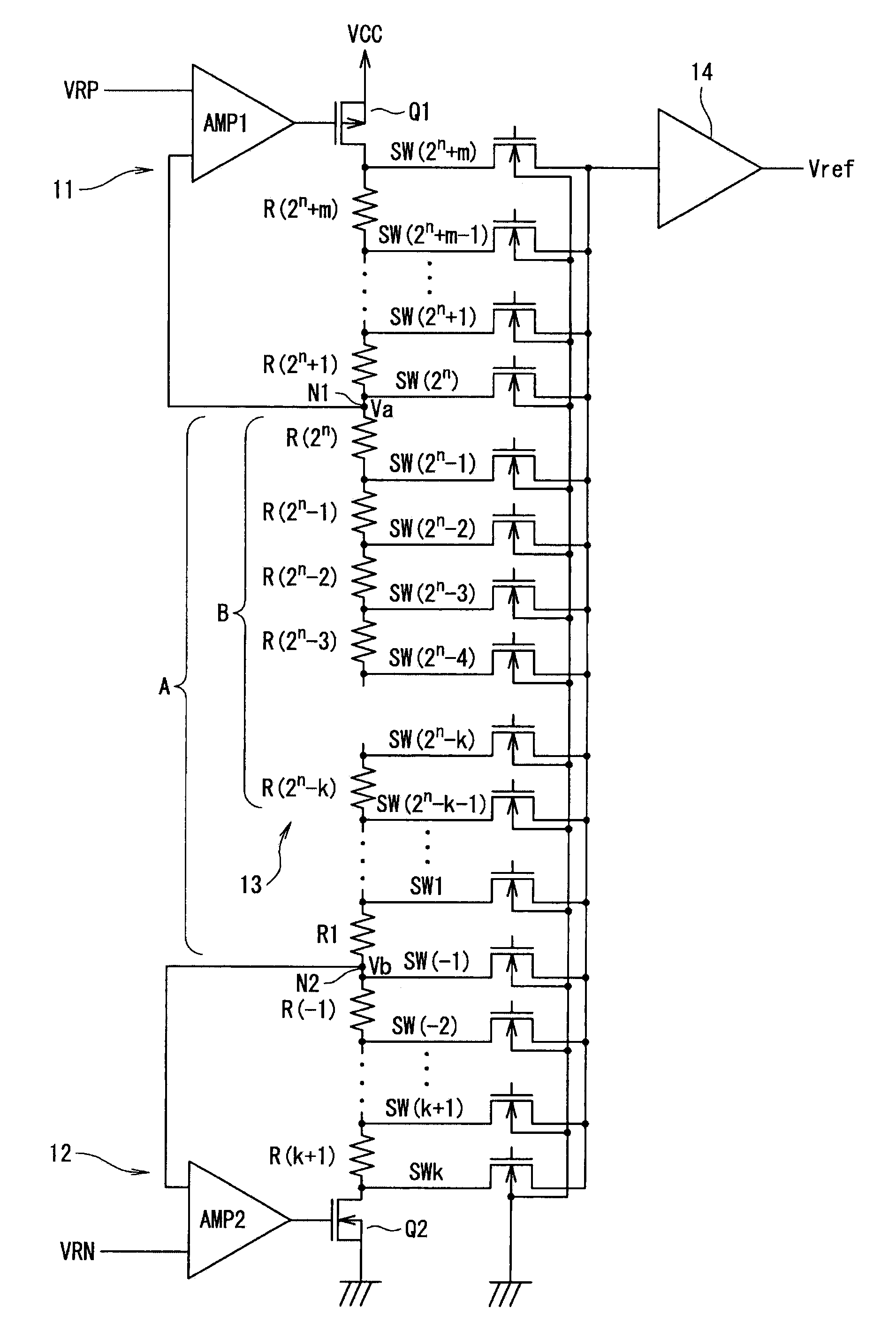
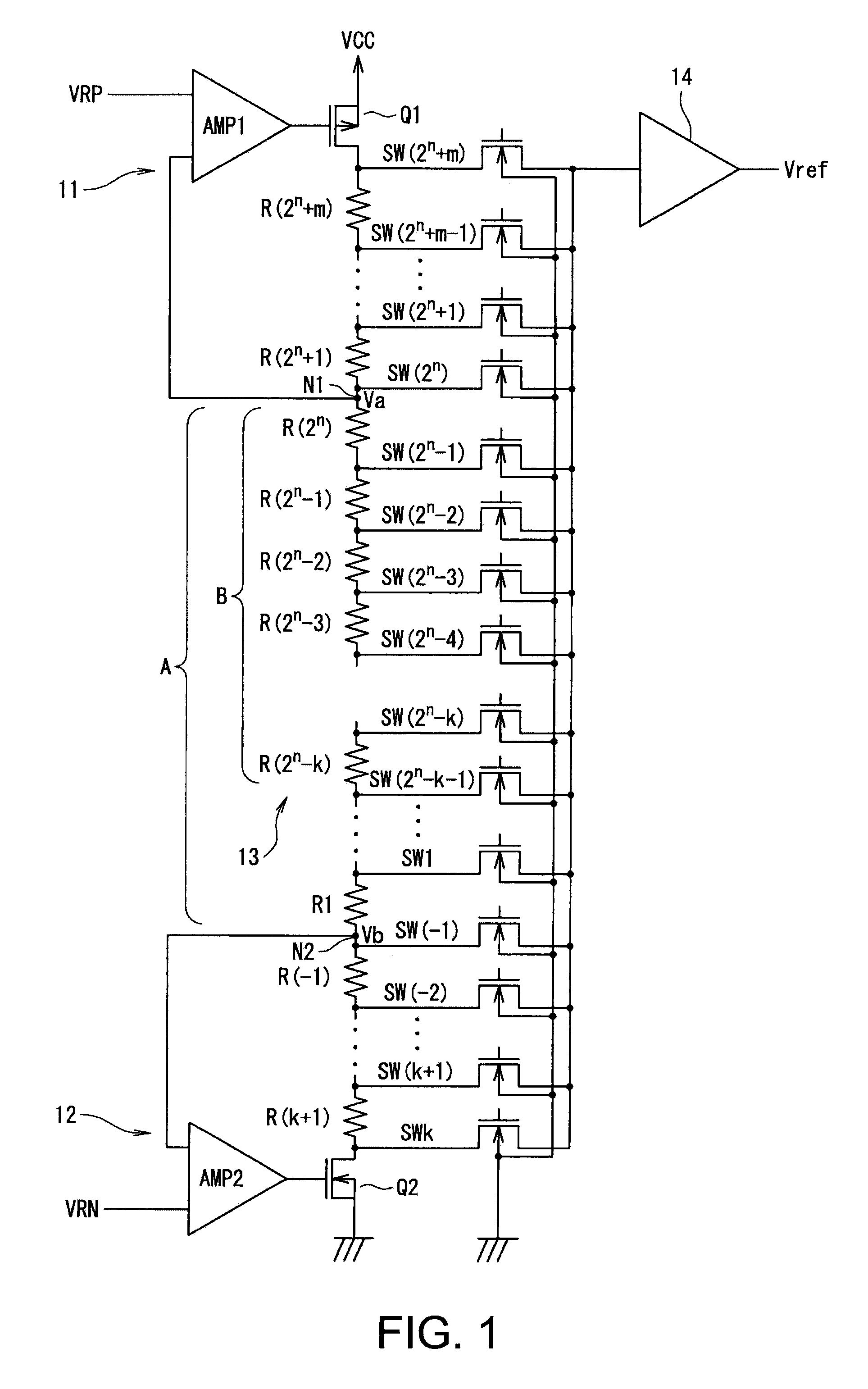
[0061]FIG. 5 is a circuit diagram showing a structure of a second embodiment of a reference voltage generation circuit of the invention. An outline of the second embodiment of the reference voltage generation circuit is explained below. An input reference voltage (for example, a voltage between a reference voltage Va at the higher side of a node N1 and a reference voltage Vb at the lower side of node N2) is divided into a plurality of divisional voltages by a plurality of resistors connected in series, one of the divisional voltages is selectively output as the reference voltage Vref by a plurality of analogue switches.
[0062]Accordingly, the second embodiment includes a first reference voltage setting circuit 21, a second reference voltage setting circuit 22, a resistor array 23 configured of a plurality of resistors RP1 to RP(2q−1), RPN, and RN1 to RN(2p−1), analogue switches SP1 to SP(2q),and SN1 to SN(2p), and a buffer circuit 24, as shown i...
PUM
 Abstract
Description
Claims
Application Information