Electrically conducting and optically transparent nanowire networks

a technology of optical transparency and nanowires, applied in the field of electric conducting and optically transparent nanowire networks, can solve the problems of brittleness of materials, limited use in certain applications, and inability to meet some (like polymeric) substrates

Inactive Publication Date: 2009-05-21
RGT UNIV OF CALIFORNIA
View PDF1 Cites 146 Cited by
  • Summary
  • Abstract
  • Description
  • Claims
  • Application Information

AI Technical Summary

Problems solved by technology

While developed to perfection, the material has nevertheless several deficiencies.
The material is deposited at high temperature, making compatibility with some (like polymeric) substrates problematic.
The difficulty in patterning, together with the sensitivity to acidic and basic environments limits the use in certain applications.
Brittleness of the material is obviously an issue for any application for which flexibility is required, and when tailored for such applications the sheet resistance is significantly higher (for the same transmittance) than an ITO film on a rigid substrate such as glass.
While a continuous ZnO film doped with Al and other metallic elements has appropriate transparency in the visible spectral range and sheet resistance (M. K. Jayaray et al Bull. Mat. Soc 25, 227 (2002), the material is brittle and thus is not appropriate for applications where mechanical flexibility is required.
While the materials have the required flexibility, they do not have the sheet resistance and transparency performance required for certain applications.
Consequently, currently there is no material that displays optical transparency and sheet resistance comparable to that of ITO on a rigid substrate, such as glass, having at the same time appropriate mechanical flexibility.

Method used


Image

  • Electrically conducting and optically transparent nanowire networks
  • Electrically conducting and optically transparent nanowire networks
  • Electrically conducting and optically transparent nanowire networks

Examples


Embodiment Construction

[0032]In describing embodiments of the present invention illustrated in the drawings, specific terminology is employed for the sake of clarity. However, the invention is not intended to be limited to the specific terminology so selected. It is to be understood that each specific element includes all technical equivalents which operate in a similar manner to accomplish a similar purpose.

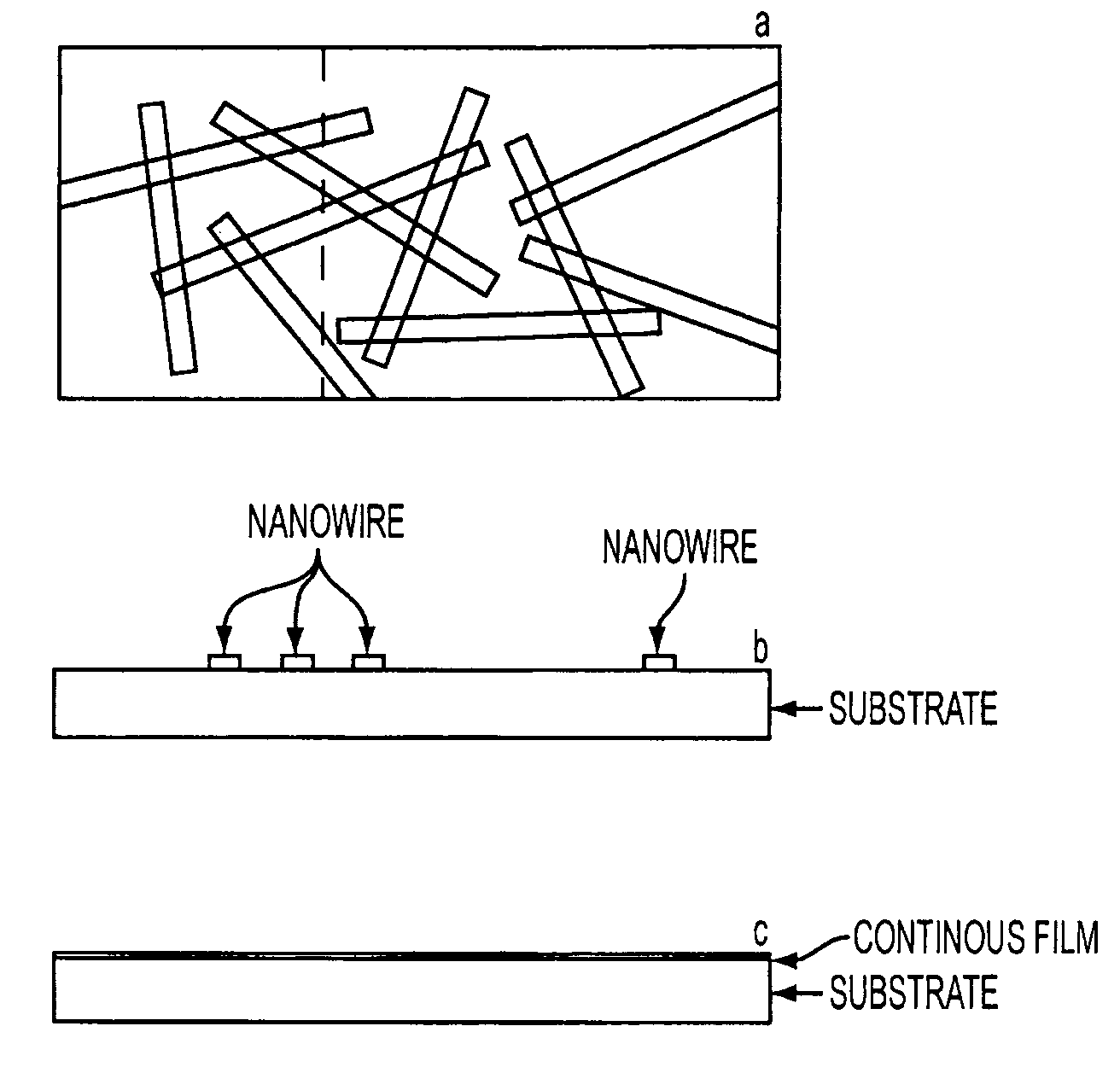
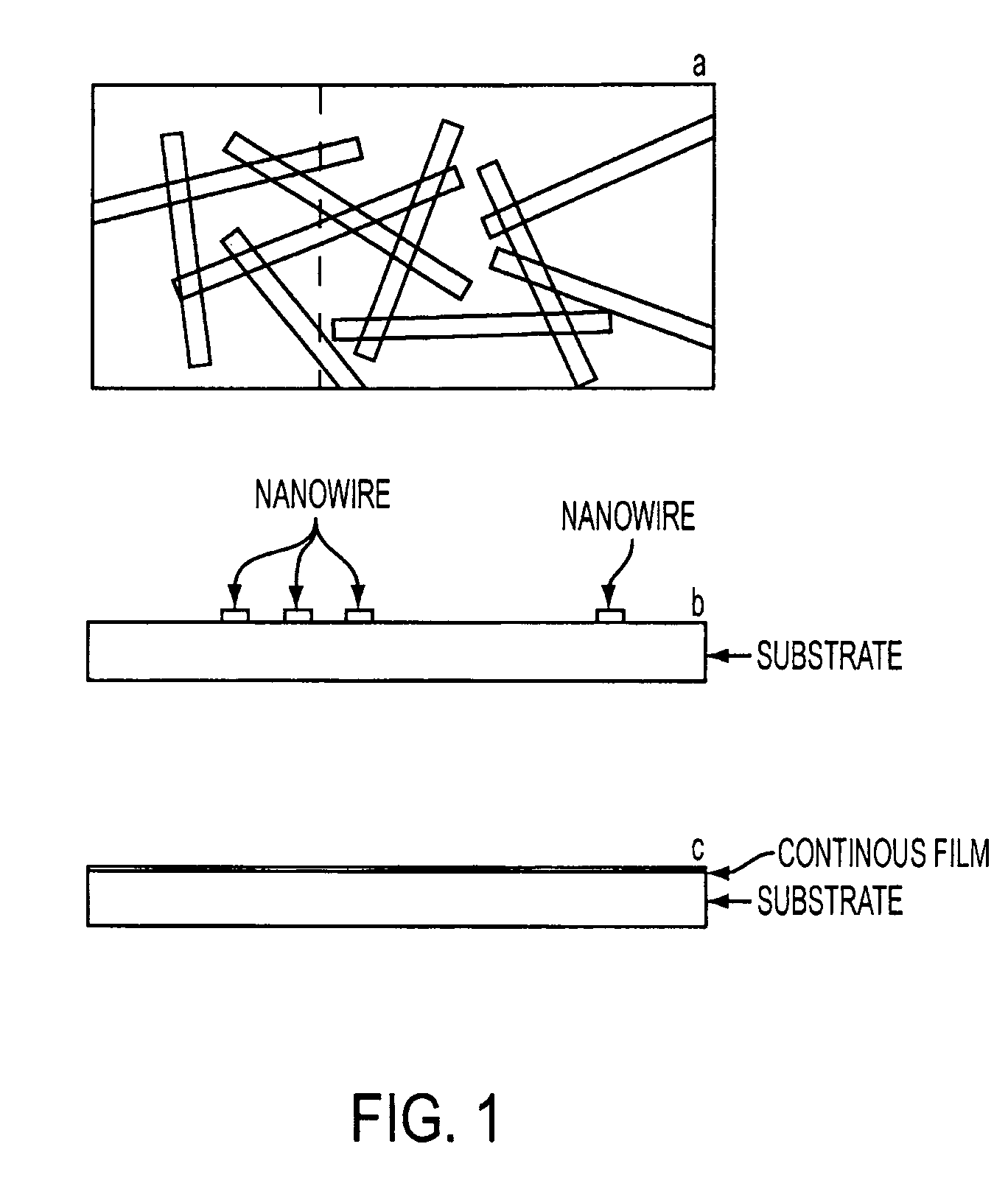
[0033]Some embodiments of the current invention are directed to a random network of transparent oxide and / or metal nanowires. An example of transparent oxide nanowires according to some embodiments of the current invention include, but are not limited to, doped ZnO. An example of metal nanowires according to some embodiments of the current invention includes, but is not limited to, silver (Ag) nanowires. A random network, while retaining the high conductivity and optical transparency also has mechanical flexibility. In addition, the one dimensional nature of the nanowires leads to increased optical tr...


PUM

PropertyMeasurementUnit
aspect ratioaaaaaaaaaa
optical transparencyaaaaaaaaaa
thicknessaaaaaaaaaa

Abstract

A network of nanowires has a plurality of interconnected nanowires. Each interconnected nanowire includes a metal in its composition. The network of nanowires is electrically conducting and substantially transparent to visible light. An electronic or electro-optic device has a network of nanowires. The network of nanowires has a plurality of interconnected nanowires, each interconnected nanowire including a metal in its composition. The network of nanowires is electrically conducting and substantially transparent to visible light. A metal-oxide nanowire has a metal oxide doped with a second metal in a composition thereof. The metal-oxide nanowire is electrically conducting and substantially transparent to visible light.

Description

CROSS-REFERENCE TO RELATED APPLICATION[0001]This application claims priority to U.S. Provisional Application No. 60 / 859,493 filed Nov. 17, 2006, the entire contents of which are hereby incorporated by reference.BACKGROUND[0002]1. Field of Invention[0003]This application relates to electrically conducting and optically transparent networks of nanowires, devices made from the nanowires and methods of production.[0004]2. Discussion of Related Art[0005]The contents of all references, including articles, published patent applications and patents referred to anywhere in this specification are hereby incorporated by reference.[0006]Various oxide materials have been used for applications where electrical conductivity and optical transparency in the visible range are required. The current choice of material for such applications is indium-tin-oxide, ITO, that provides optical transmission above 90% with a sheet resistance of less that 100 (Ohmcm)−1. While developed to perfection, the materia...

Claims


Application Information

Patent Timeline
Patent Type & Authority Applications(United States)
IPC IPC(8): H05K1/09H05K1/00G06F1/16B05D5/12H01B1/22
CPCH01L31/022466H01L31/1884H01L51/442H01L51/5206H01L2251/305H01M4/38H01L2924/0002H01M4/661H01M14/005Y02E10/549H01L2924/00H01L31/022483Y02E60/10H10K30/82H10K50/813H10K50/81H10K2102/101
Inventor GRUNER, GEORGE
Owner RGT UNIV OF CALIFORNIA
Why Eureka
Try Eureka