Semiconductor non-volatile memory

Inactive Publication Date: 2009-05-21
PANASONIC SEMICON SOLUTIONS CO LTD
View PDF13 Cites 0 Cited by
  • Summary
  • Abstract
  • Description
  • Claims
  • Application Information

AI Technical Summary

Benefits of technology

[0024]In the first conventional example, when the memory cell 04 is “1”, a part of the memory cell current flowing out of the memory cell 03 flows out to the bit line BL25 via the memory cell 04, whereby the memory cell current cannot entirely be reflected to the read voltage. In contrast, in the second conventional example, as the voltage of the bit line BL25 increases, the current flowing out of the memory cell 03 is compensated for (neighbor effect being canceled), whereby the memory cell current can effectively be transmitted to the sense amplifier input as a voltage change.
[0029]It is an object of the present invention to provide a semiconductor non-volatile memory with which a memory cell can be read accurately without having to discharge bit lines before the read operation, thereby allowing for an increase in the operation speed and a reduction in the power consumption and the circuit area.
[0031]According to the present invention, when reading the first memory cell, a predetermined voltage is applied to the first bit line connected to the drain thereof, and the second bit line connected to the source thereof is connected to the sense amplifier. The third bit line provided in the vicinity of the source of the second memory cell whose drain is connected to the second bit line is connected to the ground power supply. Thus, since the third bit line in the vicinity of the second bit line being sensed is forcibly set to the ground level, no charge flows in therefrom, thus preventing a current from flowing into the second bit line. Therefore, it is possible to accurately read the first memory cell without having to discharge bit lines before the read operation. Therefore, it is no longer necessary to provide a discharge period for discharging each bit line in the sector, whereby it is possible to increase the access speed and to eliminate the need for a circuit such as a booster power supply for the discharge operation, thus allowing for a reduction in the power consumption and the chip area.
[0033]According to the present invention, when reading the first memory cell, a predetermined voltage is applied to the first bit line connected to the drain thereof, and the second bit line connected to the source thereof is connected to the sense amplifier. The third bit line connected to the source of the second memory cell whose drain is connected to the second bit line is connected to the current source supplying a current smaller than the memory-cell-ON current. Thus, the voltage of the third bit line increases as does the voltage of the second bit line, whereby it is possible to prevent the memory-cell-ON current from leaking out to the third bit line. The fourth bit line provided in the vicinity of the source of the third memory cell whose drain is connected to the third bit line is connected to the ground power supply. Thus, since the fourth bit line in the vicinity of the third bit line is set to the ground level, no charge flows in therefrom, thus preventing a current flowing into the second bit line from the third bit line. Therefore, it is possible to accurately read the first memory cell without having to discharge bit lines before the read operation. Therefore, it is no longer necessary to provide a discharge period for discharging each bit line in the sector, whereby it is possible to increase the access speed and to eliminate the need for a circuit such as a booster power supply for the discharge operation, thus allowing for a reduction in the power consumption and the chip area.
[0034]As described above, the present invention provides a semiconductor non-volatile memory of a VGA-type, or the like, being an array configuration suitable for large-capacity applications, wherein it is no longer necessary to provide a discharge period for discharging each bit line in the sector before the read operation, whereby it is possible to shorten the cycle time, increase the access speed and to reduce the power consumption and the chip area.

Problems solved by technology

Therefore, an excessive charge on each bit line during a previous read operation needs to be collected by a somewhat complicated process.
Therefore, they are not so often used in applications where high-speed read operations are needed, and are limited to low-speed, large-capacity applications.

Method used


Image

  • Semiconductor non-volatile memory
  • Semiconductor non-volatile memory
  • Semiconductor non-volatile memory

Examples


first embodiment

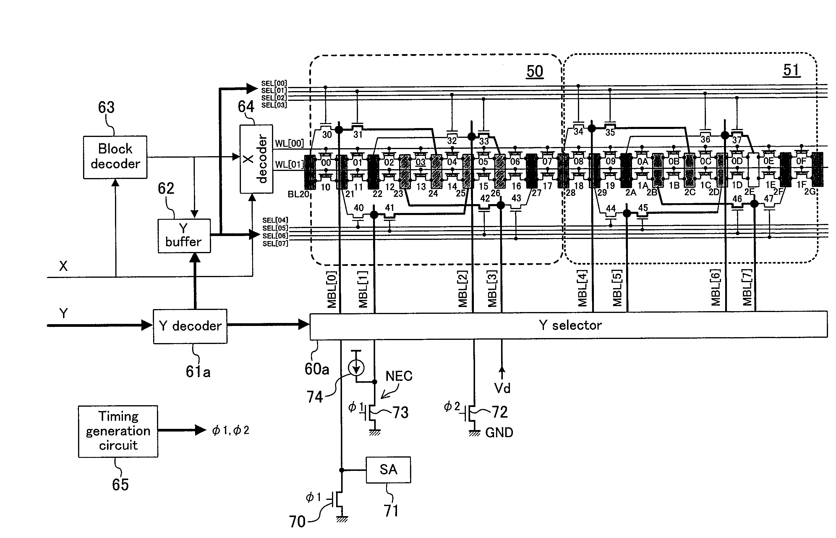
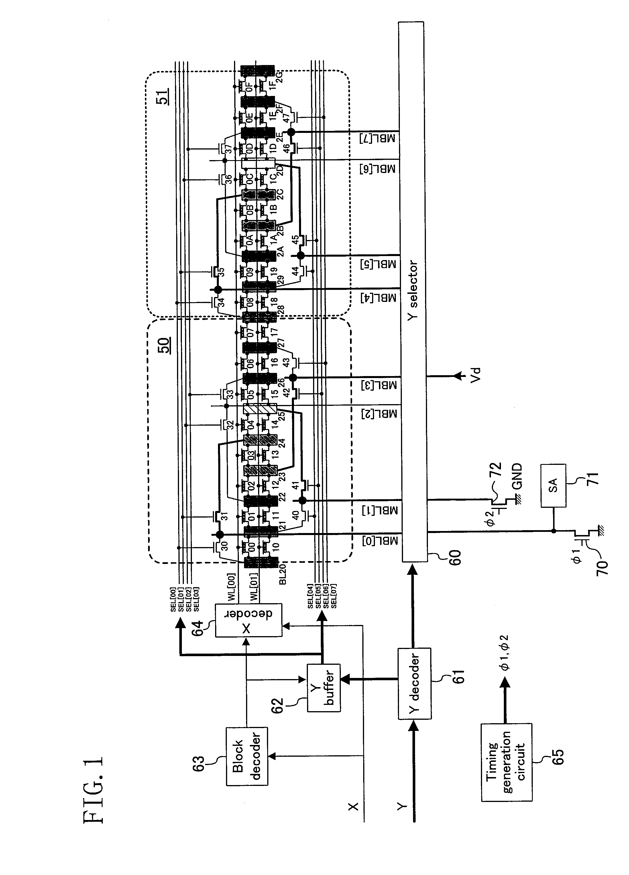
[0046]FIG. 1 shows a configuration of a semiconductor non-volatile memory according to a first embodiment of the present invention. The semiconductor non-volatile memory of FIG. 1 is a VGA (Virtual Ground Architecture)-type semiconductor non-volatile memory, including an uninterrupted arrangement of memory cells between bit lines, wherein adjacent memory cells share a bit line therebetween. Reference numerals 00 to 0F and 10 to 1F denote memory cells, reference numerals BL20 to BL2G denote bit lines, which together form a memory cell array. For example, the bit line BL24 is connected to both the source of the memory cell 03 and the drain of the memory cell 04.

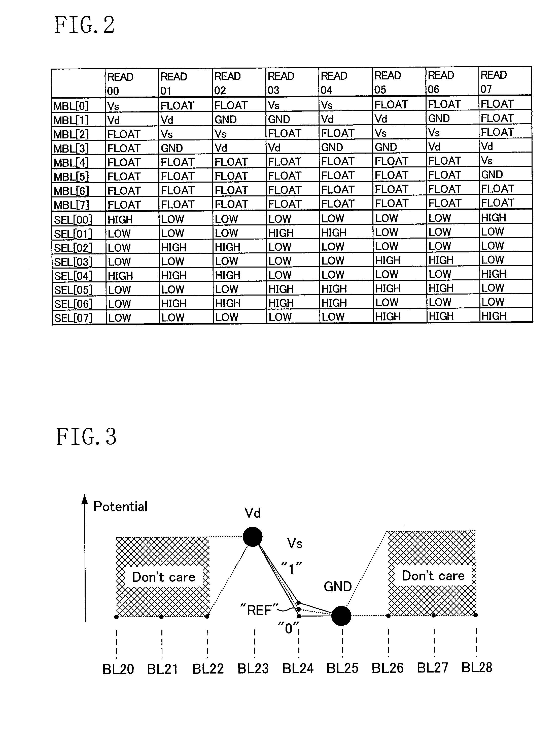
[0047]In FIG. 1, reference numerals WL[00] to WL[01] denote word lines, reference numerals MBL[0] to MBL[7] denote main bit lines, and reference numerals 30 to 37 and 40 to 47 denote selection gates selectively connecting the bit line BL20 to BL2G to the main bit lines MBL[0] to MBL[7] based on the selection gate signals SEL[00...

second embodiment

[0064]FIG. 4 shows a configuration of a semiconductor non-volatile memory according to a second embodiment of the present invention. In FIG. 4, like elements to those of FIG. 1 are denoted by like reference numerals and will not be further described below.

[0065]In addition to the configuration of FIG. 1, the semiconductor non-volatile memory of FIG. 4 includes the neighbor effect canceller section NEC as a circuit element used during a sensing operation. The neighbor effect canceller section NEC includes the neighbor bit line reset transistor 73, and the current source 74 for supplying a smaller current than the memory-cell-ON current. The current of the current source 74 is adjusted to about the same as the reference current, i.e., about one half of the current when the memory cell is “1”. The neighbor bit line reset transistor 73 receives the same control signal f 1 as that of the sense input reset transistor 70. A Y selector 60a is configured so that the main bit lines MBL[0] to ...

third embodiment

[0080]The configuration of a semiconductor non-volatile memory according to a third embodiment of the present invention is similar to that shown in FIG. 1. In the present embodiment, when reading a memory cell, a bit line that is adjacent to the drain bit line and on the opposite side of the drain bit line to the source bit line is also forcibly set to the ground potential. For example, when reading the memory cell 03, a bit line BL22 that is connected to the drain of the memory cell 02 as the third memory cell whose source is connected to the drain bit line BL23 is also connected to the ground power supply GND. Otherwise, the operation is similar to that of the first embodiment.

[0081]FIG. 7 shows potentials of bit lines in the vicinity of the memory cell 03 being read of the present embodiment, upon completion of the sense integration period. As shown in FIG. 7, the bit line BL22 adjacent to the drain bit line BL23 and on the opposite side of the drain bit line BL23 to the source b...


PUM


Abstract

A semiconductor non-volatile memory, wherein a memory cell can be read accurately without having to discharge bit lines before the read operation. When reading a memory cell, the first bit line connected to the drain thereof is connected to the voltage source to receive a predetermined voltage, and the second bit line connected to the source thereof is connected to the sense amplifier. In this process, the third bit line in the vicinity of the second bit line is connected to the ground power supply. Thus, since the third bit line in the vicinity of the second bit line being sensed is forcibly set to the ground level, no charge flows in therefrom, thus preventing a current flowing into the second bit line.

Description

CROSS REFERENCE TO RELATED APPLICATION[0001]This application claims priority under 35 U.S.C. §119 on Patent Application No. 2007-297059 filed in Japan on Nov. 15, 2007, the entire contents of which are hereby incorporated by reference.BACKGROUND OF THE INVENTION[0002]1. Field of the Invention[0003]The present invention relates to a semiconductor non-volatile memory and, more particularly, to a circuit configuration for a memory cell read operation.[0004]2. Description of the Background Art[0005]There are increasing demands for smaller sizes and larger capacities of semiconductor non-volatile memories. For high-speed applications, VGA (Virtual Ground Architecture)-type semiconductor non-volatile memories, being one type of NOR-type memories, have often been used in view of the degree of integration. A VGA-type memory includes an uninterrupted arrangement of memory cells between all bit lines, wherein adjacent memory cells share a bit line therebetween, thereby allowing for miniaturiz...

Claims


Application Information

Patent Timeline
IPC IPC(8): G11C16/04G11C16/06
CPCG11C16/26G11C16/0491
Inventor KOJIMA, MAKOTO
Owner PANASONIC SEMICON SOLUTIONS CO LTD
Why Eureka
Try Eureka