Memory System Having Multiple Vias at Junctions Between Traces

Inactive Publication Date: 2010-11-04
KK TOSHIBA
View PDF9 Cites 0 Cited by
  • Summary
  • Abstract
  • Description
  • Claims
  • Application Information

AI Technical Summary

Benefits of technology

[0011]Broadly speaking, the invention includes systems and methods for reducing the failures and capacitance associated with certain memory systems, thereby increasing the yield of the memory cells, increasing the speed with which memory cells can be read and reducing the power required by the memory system.
[0012]In one embodiment, a memory system having a hierarchical bitline structure includes an improvement wherein traces that form global write lines are connected to each other using junctions that include multiple vias, thereby reducing the capacitance associated with these lines. Further, if one of the vias fails, the remaining via(s) still provide a good connection between traces. At least one of a pair of traces connected by the vias includes a widened portion that provides sufficient overlap with the other of the pair of traces to allow the two or more vias to be formed between the traces at the overlap. Parallel traces for global write lines that carry a write signal and its inverse may be positioned more than one maximum-density grid space apart to allow the widened portions to be formed between the traces. A global read line that is formed in a different metal layer from the global write line traces may be positioned in a grid space between the global write line traces to reduce the capacitance of this line.
[0014]In one embodiment, traces of two different global write lines are formed next to each other in the same metal layer. The traces are not positioned at the minimum spacing allowable, but are separated to provide additional space between them. The traces are widened by forming bumpouts that extend into the space between the traces. The bumpouts provide the additional overlap between these traces and traces in a different metal layer so that multiple-via junctions can be formed between the traces in the different metal layers. The space can also be used to position a global read line (which is in a different metal layer from the global write lines), which may reduce the capacitance of the global read line.
[0016]The various embodiments of the present invention may provide a number of advantages over the prior art. In particular, the present systems and methods may reduce the capacitance of lines such as the global write lines of a memory system utilizing a hierarchical bit line scheme, thereby increasing their access speed in comparison to conventionally configured systems. The present systems and methods may also increase the yield of memory cells because the additional vias in a connection between traces may maintain a good connection even when one of the vias fails. The present systems and methods may also read reduce the capacitance of a global read line of a hierarchical bit line memory system, resulting in increased access speed. The reductions in capacitance using the present systems and methods may also result in reduced power consumption.

Problems solved by technology

There are, however, physical limitations to some of these techniques.
For instance, the frequency of the clock signal used in a digital circuit cannot be increased beyond the point at which the components that use the clock signal become unstable.
Similarly, a power supply voltage cannot be reduced to a level at which the components operating on this supply voltage no longer function properly, and the physical size of a circuit components cannot be reduced to a size which is too small to be resolved using available process technologies.
As a result of the current leaks in all of the cells connected to the bit line, it can be difficult to reliably read data from a single one of the cells.
Because of the connections between metal traces that form the system and the close proximity of some of the traces in the conventional system, there is capacitance which reduces the maximum speed at which the cells can be operated and also increases the power required to operate the cells.
Additionally, the vias that connect the traces may fail, causing the memory cells to fail.

Method used


Image

  • Memory System Having Multiple Vias at Junctions Between Traces
  • Memory System Having Multiple Vias at Junctions Between Traces
  • Memory System Having Multiple Vias at Junctions Between Traces

Examples


Embodiment Construction

[0026]One or more embodiments of the invention are described below. It should be noted that these and any other embodiments described below are exemplary and are intended to be illustrative of the invention rather than limiting.

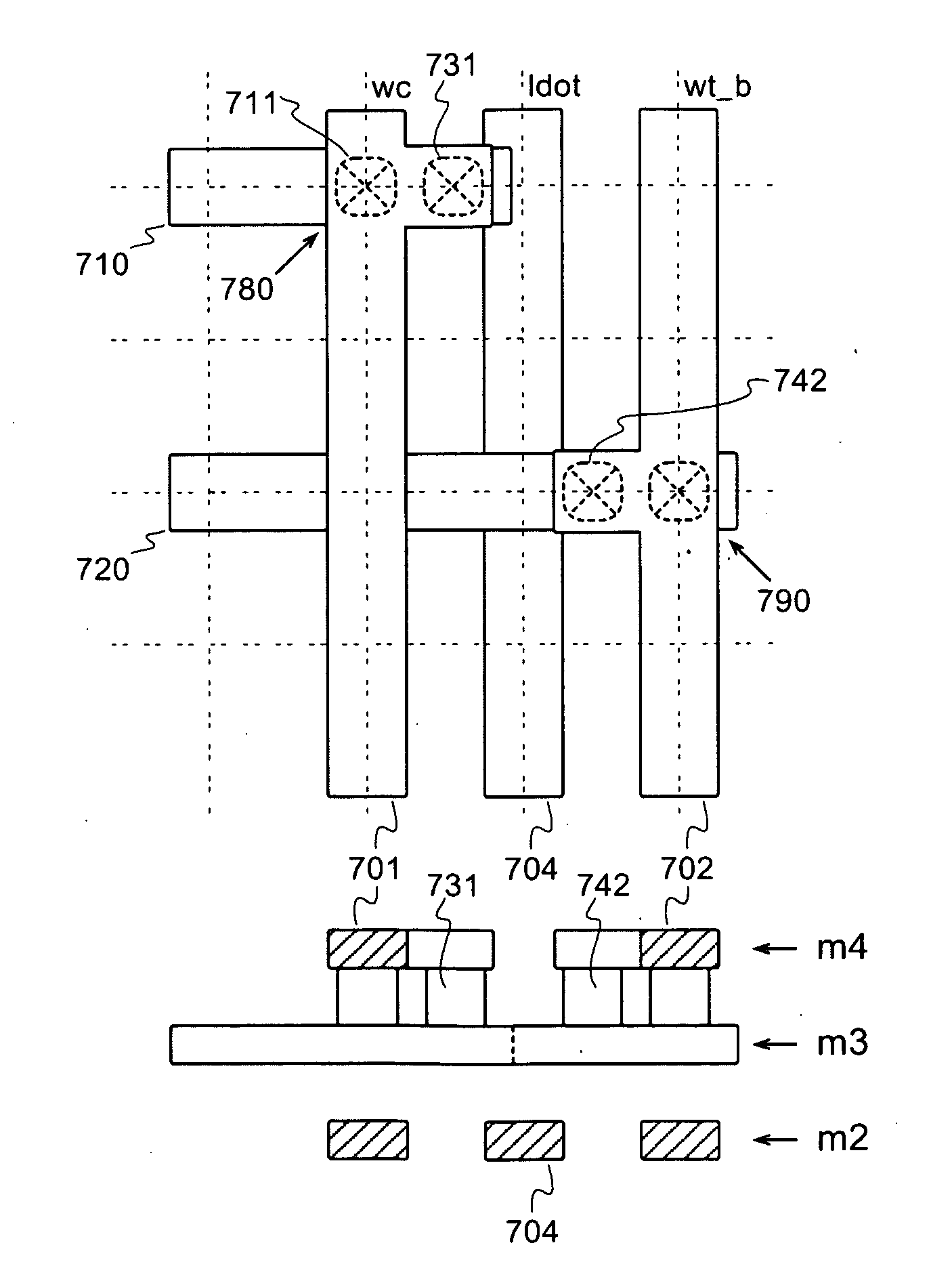
[0027]Broadly speaking, the invention includes systems and methods for increasing the yield and reducing the capacitance associated with memory system circuits, thereby potentially increasing the speed and reducing the power required by these systems. More particularly, the system is improved by introducing additional vias between the traces of different metal layers.

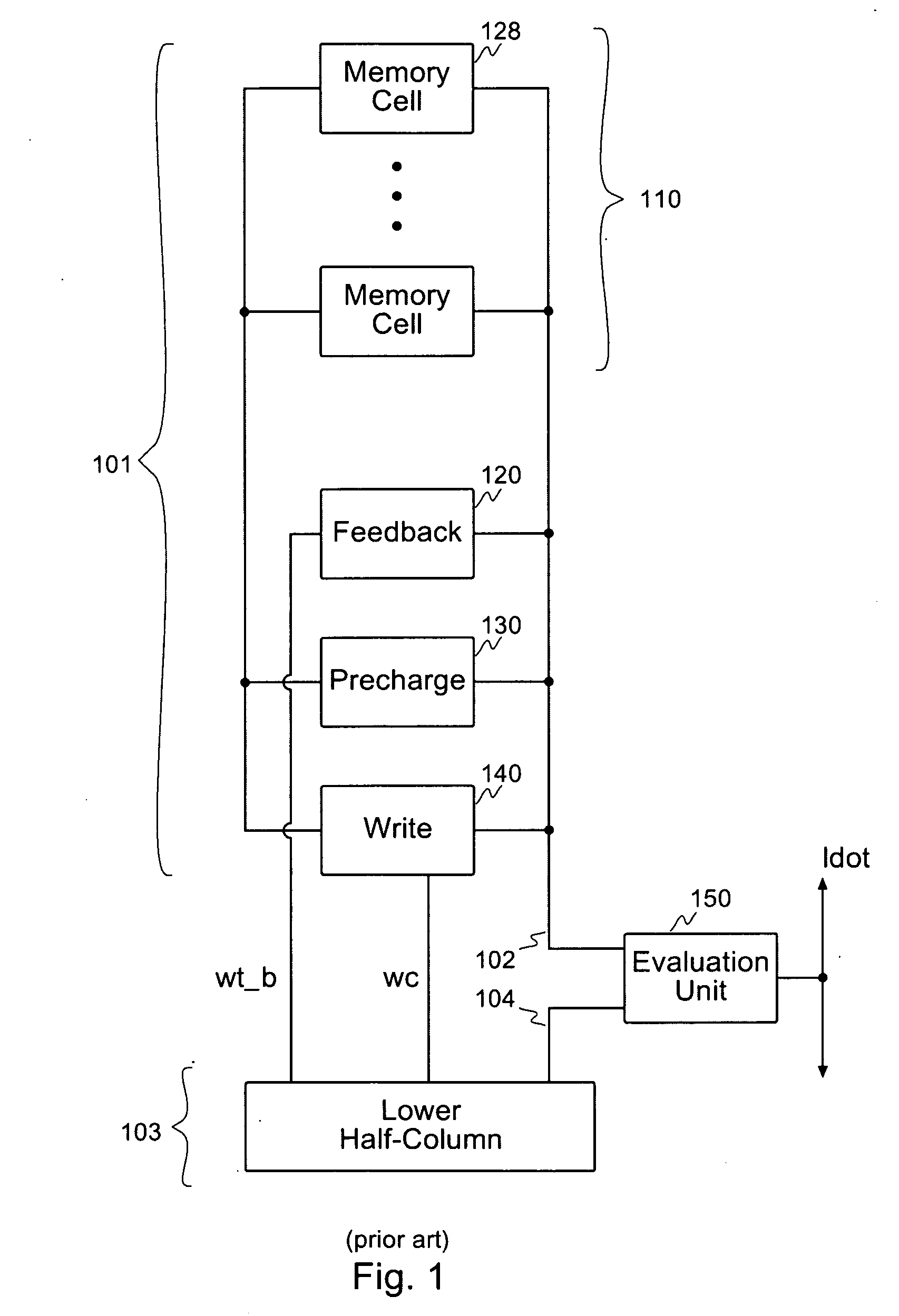
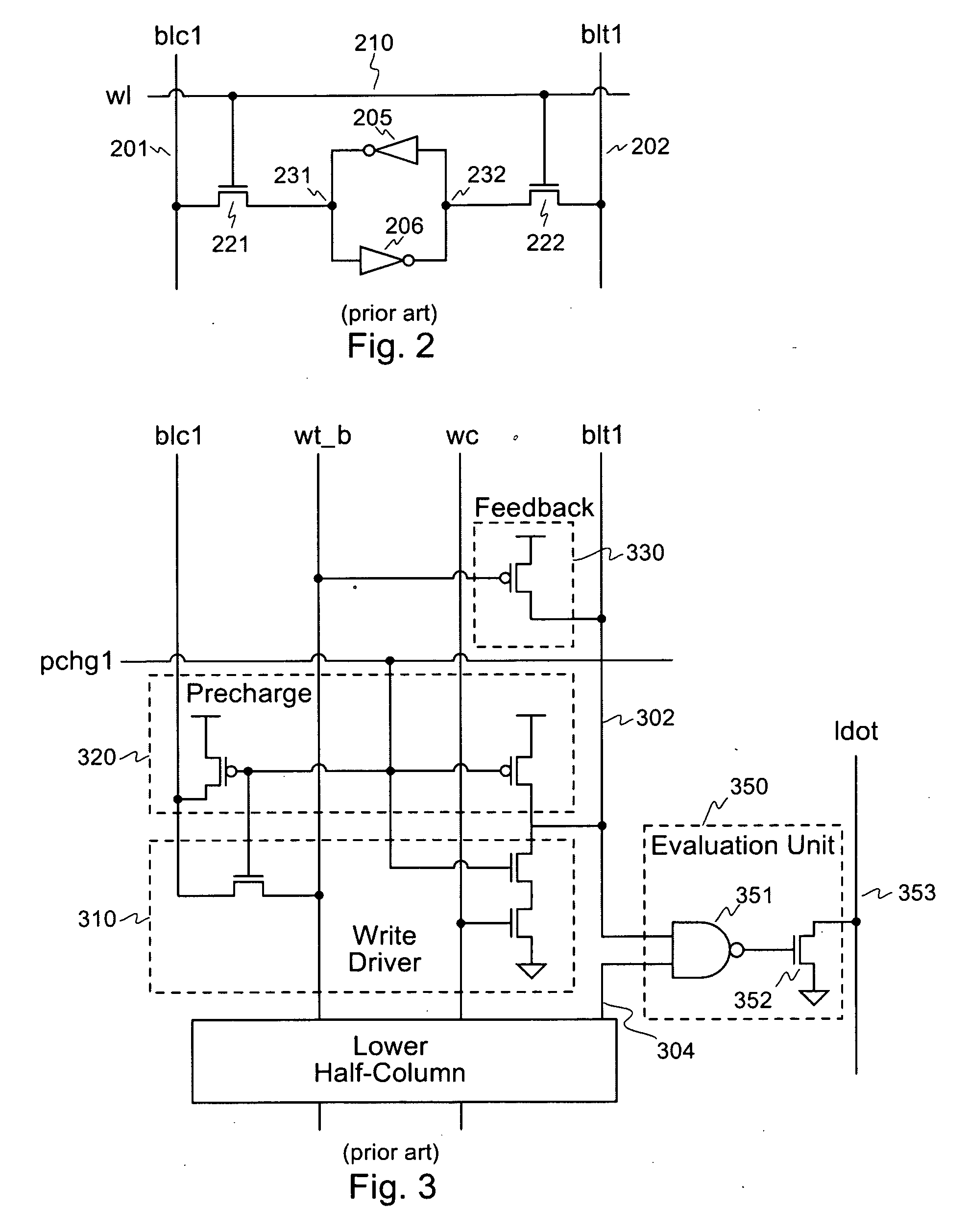
[0028]An exemplary embodiment is implemented in a memory system that uses a hierarchical bit line scheme. The capacitance of some of the lines in the memory system can be reduced by adding vias between metal layers. In one embodiment, a set of SRAM memory cells is organized in an array wherein each cell is accessed / read by a bit line. Each memory cell is connected to the bit line at a correspondi...


PUM

PropertyMeasurementUnit
Densityaaaaaaaaaa
Widthaaaaaaaaaa

Abstract

An improvement to a memory system having a hierarchical bitline structure wherein traces that form global write lines are connected to each other using junctions that include multiple vias to reduce capacitance and increase yield. At least one of a pair of traces connected by the vias includes a widened portion that provides sufficient overlap with the other trace to allow the two or more vias to be formed between the traces at the overlap. Parallel traces for global write lines that carry a write signal and its inverse may be positioned more than one maximum-density grid space apart to allow the widened portions to be formed between the traces. A global read line that is formed in a different metal layer from the global write line traces may be positioned in a grid space between the global write line traces to reduce the capacitance of this line.

Description

BACKGROUND [0001]1. Field of the Invention[0002]The invention relates generally to memory systems, and more particularly to systems and methods for reducing the capacitance associated with certain memory systems thereby increasing the speed with which memory cells can be read and reducing the power required by the memory system.[0003]2. Related Art[0004]There is a continuing demand in the design of electronic circuits for increased computational power and decreased size and power consumption. These goals are achieved in various ways, such as by improving the physical characteristics of the devices. For example, computational power may be increased by developing components that can operate at higher clock speeds than previous components. Device size may be reduced by using technologies that allow smaller features to be constructed on an integrated circuit die. Lower power consumption may be achieved by using lower power supply voltages. Many other techniques are also used to meet the...

Claims


Application Information

Patent Timeline
IPC IPC(8): G11C5/06G11C7/00
CPCG11C5/063G11C7/12G11C7/18Y10T29/49117H01L27/11H01L27/1116H01L27/1052H01L27/105H10B99/00H10B10/00H10B10/18
Inventor KONO, FUMIHIRO
Owner KK TOSHIBA
Why Eureka
Try Eureka