Development device and development method

a technology of developing apparatus and developing method, which is applied in the direction of photosensitive materials, instruments, cleaning using liquids, etc., can solve the problems of increasing the manufacturing cost of semiconductor devices, consuming a large amount of developing solution, and suffering above the developing method, so as to reduce the amount of developing solution and short time

Active Publication Date: 2009-05-21
TOKYO ELECTRON LTD
View PDF11 Cites 51 Cited by
  • Summary
  • Abstract
  • Description
  • Claims
  • Application Information

AI Technical Summary

Benefits of technology

[0008]The present invention has been made in view of the above problems. It is, therefore, an object of the present invention to provide an...

Problems solved by technology

However, the above developing method suffers from the following problem.
To overcome this problem, a large amount of developing solution must be supplied to the surface of the wafer W. However, this consumes a large amount of developing solution, increasing the manufacturing cost of the semiconductor device.
However, if the size of the ejection port of the developer nozzle is reduced to reduce the amount of developing solution consumed, it takes a long time to apply a developing solution to the entire surface of the wafer W, resulting in increase of the developing time.
Furthermore, different portions of the wafer W may be in contact with the developing solution for different amount...

Method used


Image

  • Development device and development method
  • Development device and development method
  • Development device and development method

Examples


Embodiment Construction

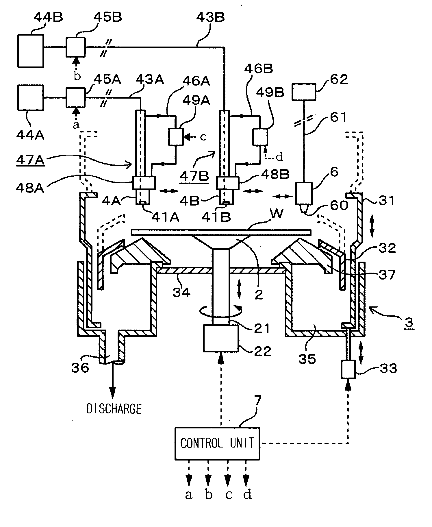
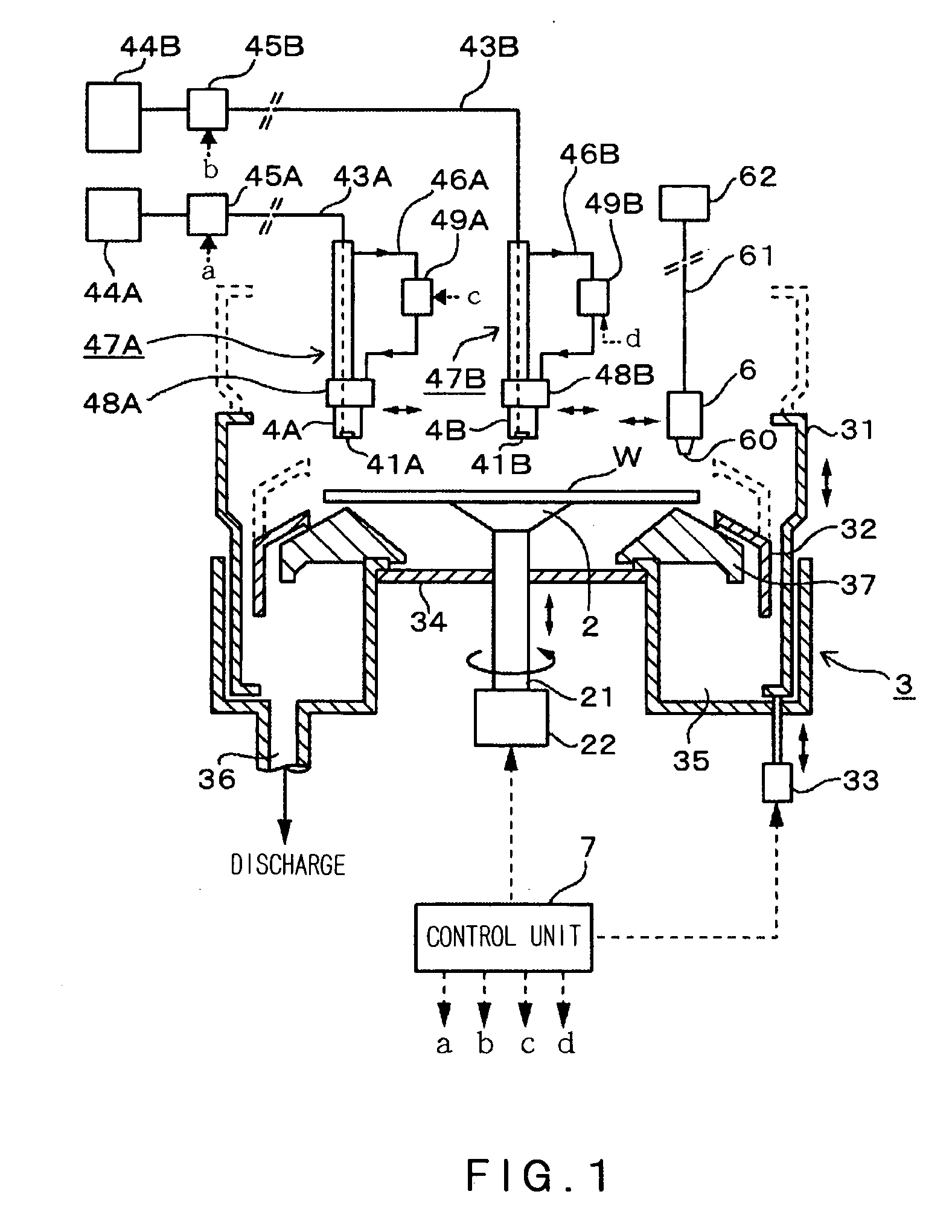
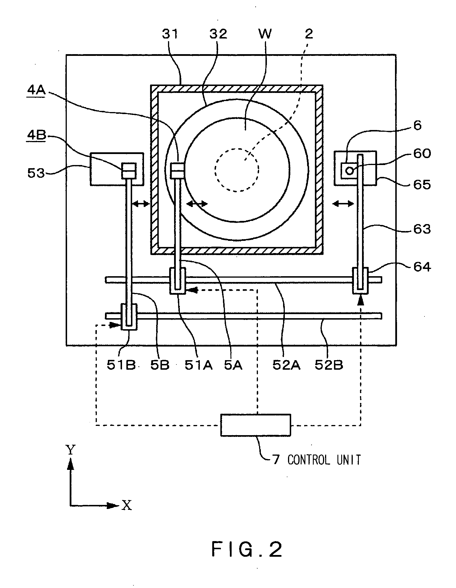
[0042]A developing apparatus in one embodiment of the present invention will be described with reference to FIGS. 1 and 2. Reference numeral 2 denotes a spin chuck (i.e., a substrate holding unit) for holding a substrate (e.g., a wafer W) in a horizontal attitude by holding the center portion of the back side of the substrate by suction. The spin chuck 2 is connected to a drive mechanism 22 through a rotational shaft 21 and can be rotated, raised and lowered together with the wafer W held thereon, by the drive mechanism 22. In the illustrated embodiment, the wafer W is set on the spin chuck 2 such that the center of the wafer W is located on the rotational axis line of the spin chuck 2. However, in the present invention, the center of the wafer W need not necessarily be positioned on the rotational axis. The center of the wafer W may be located in a circular region of a radius in a range of 1 to 15 mm centered about the rotational axis.

[0043]A cup set 3 is provided so as to surround...


PUM


Abstract

A developer nozzle is moved from a periphery of a wafer toward the central portion while an exposed substrate held at a spin chuck is being rotated about a vertical axis and while a developing solution is being discharged from the developer nozzle, and this way the developing solution is supplied to the surface of the wafer, the developer nozzle having a slit-like ejection port whose longitudinal direction is oriented to the direction perpendicular to the radial direction of the wafer. The movement speed of the nozzle is higher than a case where a nozzle with a small-diameter circular nozzle is used, and this enables a development time to be reduced. Further, the thickness of a developing solution on a substrate can be reduced, so that the developing solution can be saved.

Description

TECHNICAL FIELD[0001]The present invention relates to a developing apparatus and method for developing an exposed resist on a substrate surface.BACKGROUND ART[0002]A semiconductor manufacturing process includes a photoresist process in which a resist is coated onto the surface of a semiconductor wafer (hereinafter referred to simply as a wafer), exposed in a predetermined pattern, and then developed to form a resist pattern. Such a process is generally performed by a system in which a coating-and-developing apparatus for coating-and-developing a resist is connected to an exposure apparatus.[0003]The operation of the developing apparatus disclosed in JP7-263302A will be described with reference to FIG. 17. First, a wafer W is held in a horizontal attitude on a spin chuck 1, and a developer nozzle 11 is positioned such that its small diameter ejection port is located slightly higher than the surface of the wafer W. Then, the developer nozzle 11 is moved in a radial direction relative ...

Claims


Application Information

Patent Timeline
IPC IPC(8): G03C5/00G03G15/10G03F7/30H01L21/00H01L21/027
CPCG03F7/3021H01L21/67051Y10S134/902H01L21/6715H01L21/6719H01L21/6708H01L21/02057
Inventor OOKOUCHI, ATSUSHIYAMAMOTO, TAROTAKEGUCHI, HIROFUMIKYOUDA, HIDEHARUYOSHIHARA, KOUSUKE
Owner TOKYO ELECTRON LTD
Why Eureka
Try Eureka