
Range pattern definition of susceptibility of layout regions to fabrication issues

a layout region and pattern technology, applied in the field of layout design, can solve the problems of fabricated wafers, unable to overcome such fabrication problems, and reducing the fidelity of reticle enhancement technologies such as optical proximity correction (opc), phase shifting masks (psm),

Active Publication Date: 2009-05-21
SYNOPSYS INC
View PDF34 Cites 17 Cited by
  • Summary
  • Abstract
  • Description
  • Claims
  • Application Information

AI Technical Summary

Benefits of technology

The invention is a computer program that uses a data structure called a range pattern to represent the arrangement of line segments in an integrated circuit (IC) layout. This range pattern includes information about the position and size of the line segments. By using a single range pattern, the program can compactly represent numerous patterns that are similar in many ways but differ in the position of a small number of line segments. This eliminates the need for separate representations of each pattern, saving memory space. The range pattern includes information about the maximum and minimum limits of a line segment, which helps identify regions in the layout that may have fabrication issues. Overall, the invention simplifies the process of creating and analyzing IC layouts.

Problems solved by technology

Accordingly it has become increasingly difficult to achieve reasonable fidelity (including resolution and depth of focus) between (a) a layout as designed in a computer and (b) shapes of circuit elements formed in a wafer after fabrication (which normally involves a number of processes such as photolithography followed by Cu deposition and chemical mechanical polishing).
A number of reticle enhancement technologies (RET) such as optical proximity correction (OPC), phase shifting masks (PSM), and sub-resolution assist features (SRAF) are unable to overcome such fabrication issues.
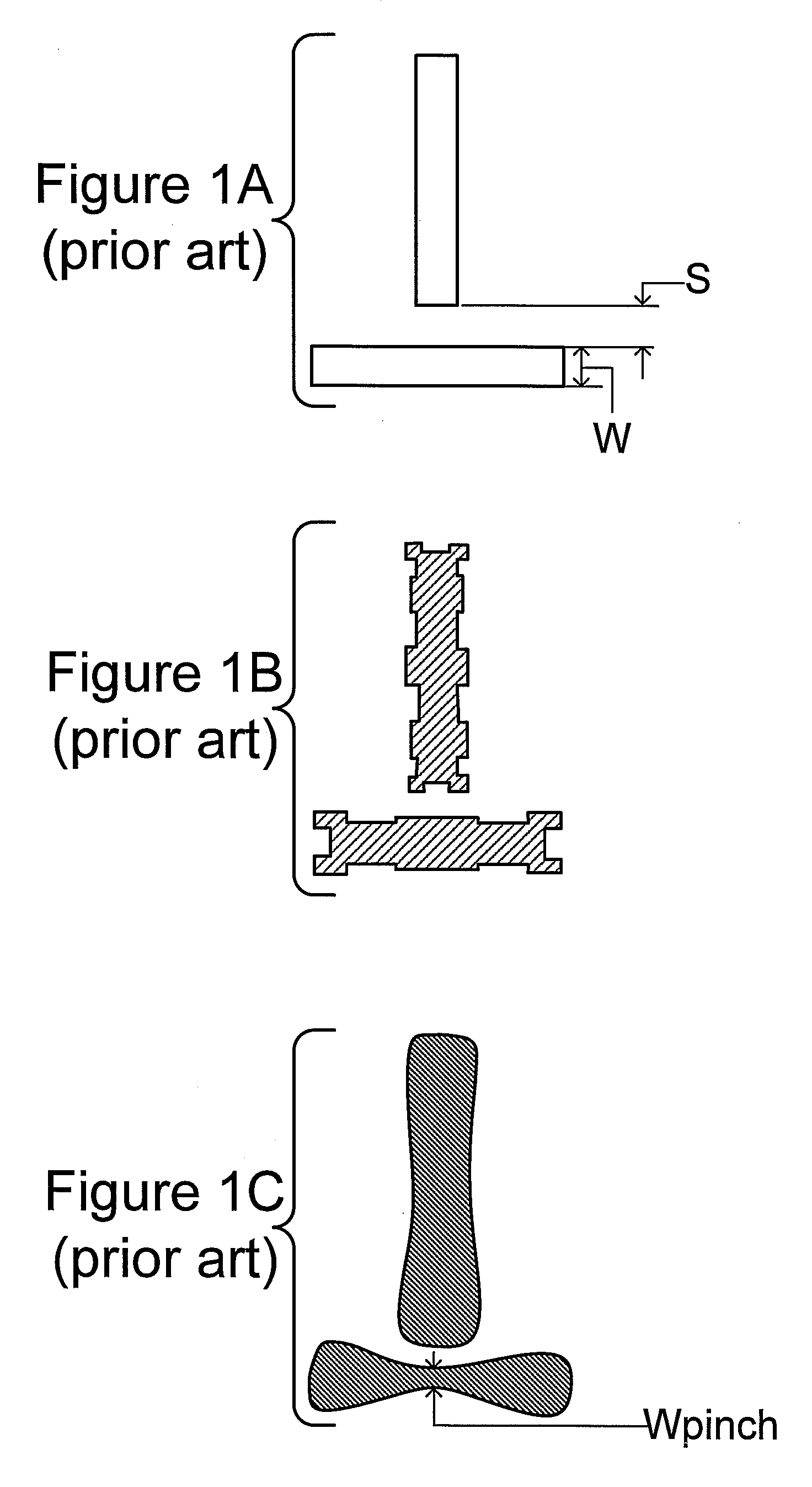
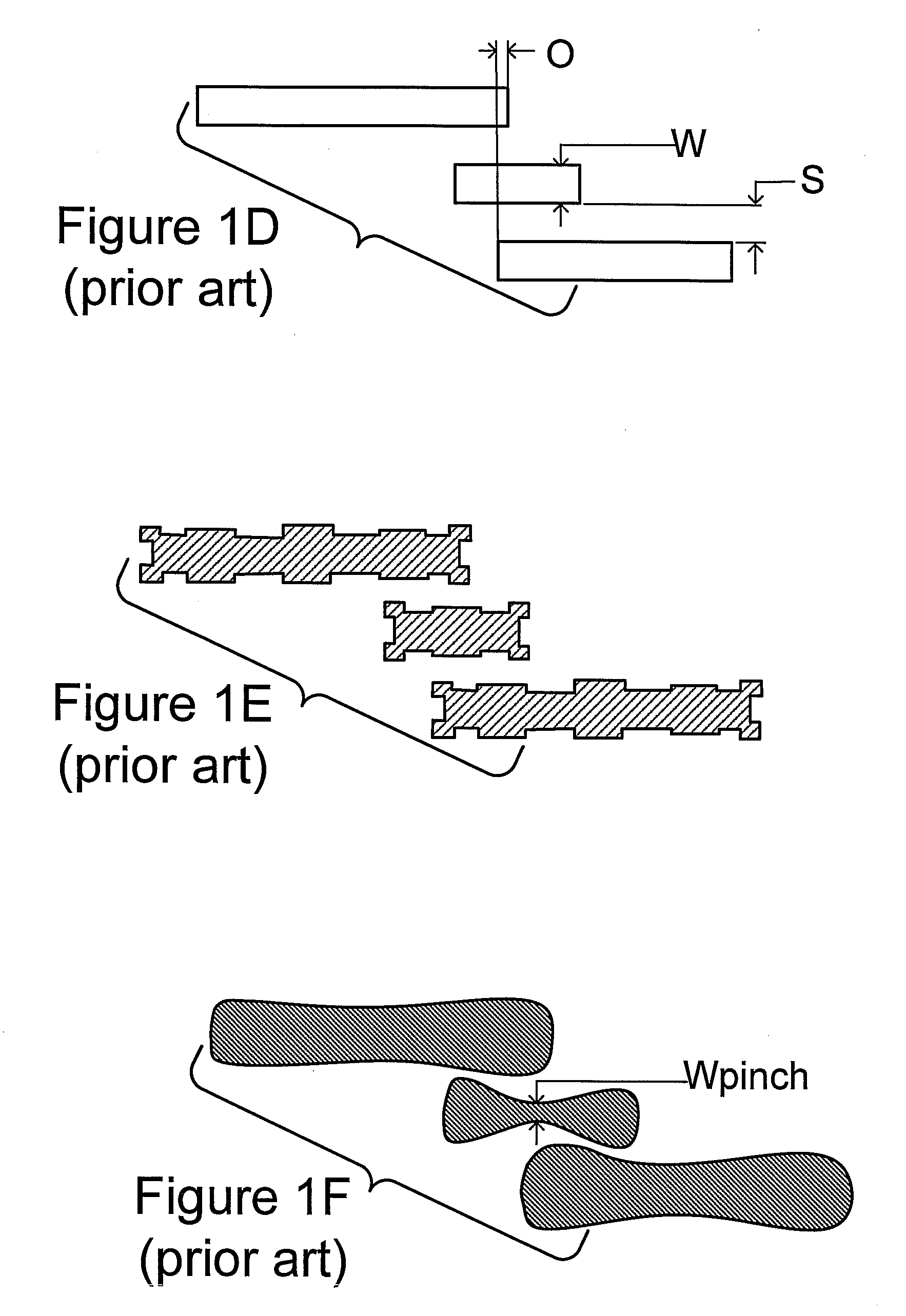
For example, even after a layout (FIG. 1A and FIG. 1D) is OPC corrected (FIGS. 1B and 1E), the resulting shape in a fabricated wafer (FIGS. 1C and 1F) may have one or more defects (e.g. Wpinch falls below a minimum limit, and causes an open circuit failure in the IC chip).
However, use of such fab-specified design rules can result in over-specification of the design or an unnecessarily large number of defects from fabrication thereby reducing yield.
Since it is very time consuming to accurately estimate the amount of RET that a particular routed layout needs without performing the actual operation on designs (performing RET takes about 20-30 hours of simulation time for a 1-million gate design, when using a personal computer (PC) with a central processing unit (CPU) operating at 1 GHz and equipped with 1 GB memory), such methods typically use a simple aerial image simulator to find geometric shapes in the layout that are expected to print badly.
Consequently, these methods lack the ability to factor in RET information when identifying potential hotspots.
Correcting all the tagged hotspots in the layout routing stage results in overly-conservative, less than optimal routing design.

Method used


Image

  • Range pattern definition of susceptibility of layout regions to fabrication issues
  • Range pattern definition of susceptibility of layout regions to fabrication issues
  • Range pattern definition of susceptibility of layout regions to fabrication issues

Examples


Embodiment Construction

[0055]A computer, when appropriately programmed in accordance with the invention, contains in memory at least one data structure to represent numerous patterns compactly. The data structure (called “range pattern”) typically identifies the relative location of pairs of line segments in the patterns using a range, such as a width range for a rectangle in the pattern, as illustrated in FIG. 2A. In the example illustrated in FIG. 2A, a range pattern 200 represents an arrangement of two traces oriented perpendicular to one another, in the form of an inverted letter “T” of the English Alphabet with the two traces separated from one another by a spacing distance S. The horizontal trace in this example is represented in range pattern 200 by a rectangle 201 of fixed dimensions. The vertical trace in this example is represented by a rectangle 202 of fixed length L but the width of rectangle 202 can be any value within the range (called “width range”) defined by two values, namely a minimum l...


PUM


Abstract

A memory is encoded with a data structure that represents a pattern having a range for one or more dimensions and / or positions of line segments therein. The data structure identifies two or more line segments that are located at a boundary of the pattern. The data structure also includes at least one set of values that identify a maximum limit and a minimum limit (i.e. the range) between which relative location and / or dimension of an additional line segment of the pattern in a portion of a layout of an integrated circuit (IC) chip, represents a defect in the IC chip when fabricated. In most embodiments, multiple ranges are specified in such a range defining pattern for example a width range is specified for the width of a trace of material in the layout and a spacing range is specified for the separation distance between two adjacent traces in the layout.

Description

CROSS-REFERENCE TO PARENT APPLICATION[0001]This application is a divisional application of U.S. patent application Ser. No. 11 / 394,466 filed on Mar. 31, 2006 entitled “A RANGE PATTERN DEFINITION OF SUSCEPTIBILITY OF LAYOUT REGIONS TO FABRICATION ISSUES” by Subarnarekha Sinha and Charles C. Chiang. U.S. patent application Ser. No. 11 / 394,466 is incorporated by reference herein in its entirety.CROSS-REFERENCE TO RELATED APPLICATION[0002]This application is related to and incorporates by reference herein in its entirety U.S. patent application Ser. No. 11 / 395,006 entitled “IDENTIFYING LAYOUT REGIONS SUSCEPTIBLE TO FABRICATION ISSUES BY USING RANGE PATTERNS” filed on Mar. 31, 2006 by Subarnarekha Sinha, Hailong Yao, and Charles C. Chiang.BACKGROUND[0003]1. Field of the Invention[0004]The invention relates to design of layouts used in fabrication of semiconductor wafers. More specifically, the invention relates to a method and an apparatus for representing several patterns, which are sim...

Claims


Application Information

Patent Timeline
Patent Type & Authority Applications(United States)
IPC IPC(8): G06F17/50
CPCG03F1/144G06F17/5081G03F1/36G06F30/398
Inventor SINHA, SUBARNAREKHACHIANG, CHARLES C.
Owner SYNOPSYS INC
Learn More