Semiconductor range-finding element and solid-state imaging device

a technology of solid-state imaging and electromagnetic field, which is applied in the direction of reradiation control devices, instruments, etc., can solve the problems of shooting noise causing the drop in range measurement precision, the inability of range-finding sensors and the inability to effectively reduce the influence of background light. achieve the effect of wide dynamic range, wide range measurement precision, and wide maximum range measurement coverag

Active Publication Date: 2009-05-28
NAT UNIV CORP SHIZUOKA UNIV +1
View PDF4 Cites 44 Cited by
  • Summary
  • Abstract
  • Description
  • Claims
  • Application Information

AI Technical Summary

Benefits of technology

[0006]It is an object of the present invention to provide a TOF type semiconductor range-finding element, by effectively reducing the influence of a background light, which has a high range measurement precision (distance resolution),

Problems solved by technology

However, the earlier TOF range-finding sensors could not effectively reduce the influence of background light.
Thus, when there are bias charges caused by the background light, the shot noise causes the drop in a range measurement precision.
When the dynamic range is assumed to be represented by the maximum value for the signal and the noise level, the increase in the noise leads to the decrease in

Method used


Image

  • Semiconductor range-finding element and solid-state imaging device
  • Semiconductor range-finding element and solid-state imaging device
  • Semiconductor range-finding element and solid-state imaging device

Examples


first embodiment

Modification of First Embodiment

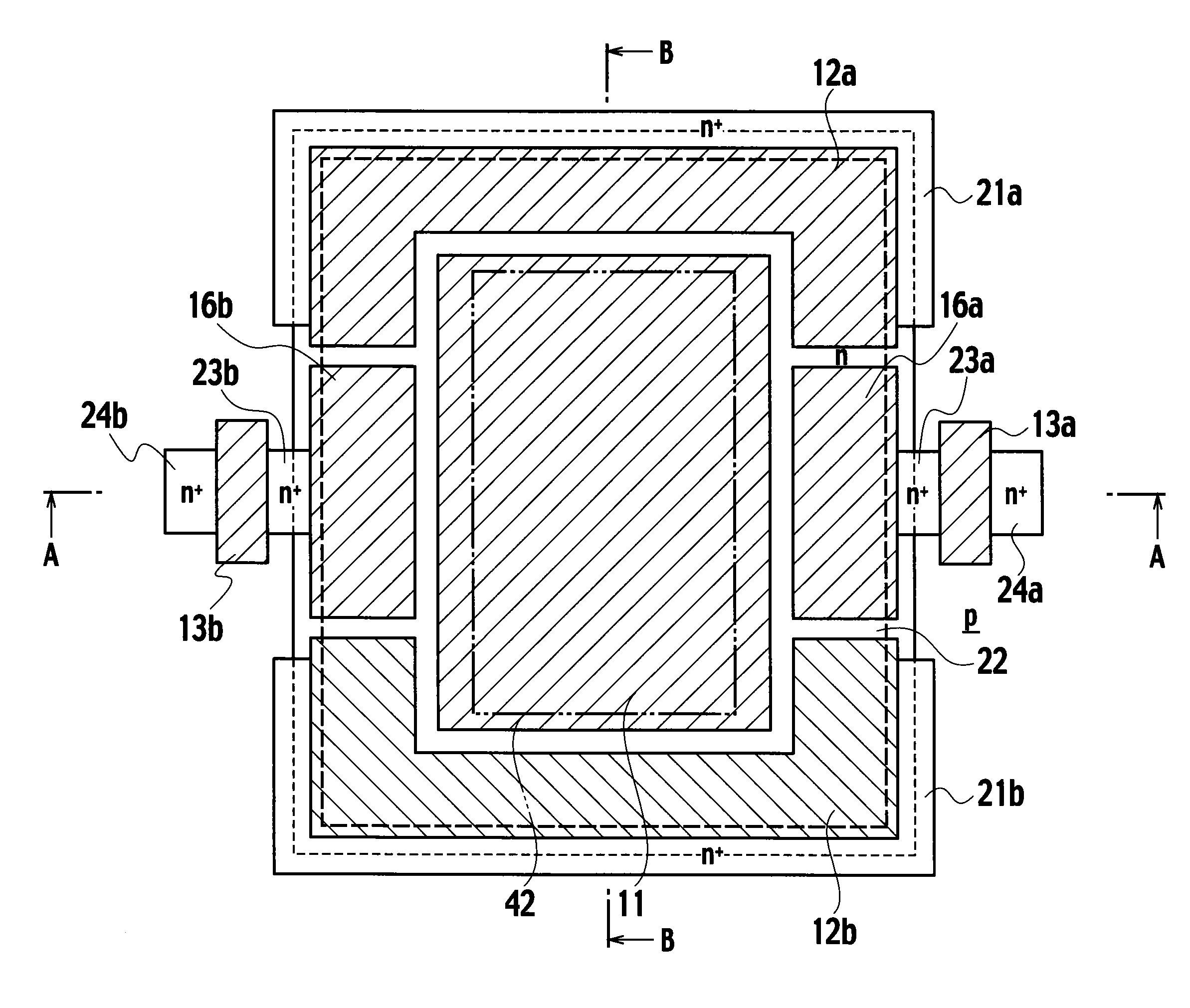
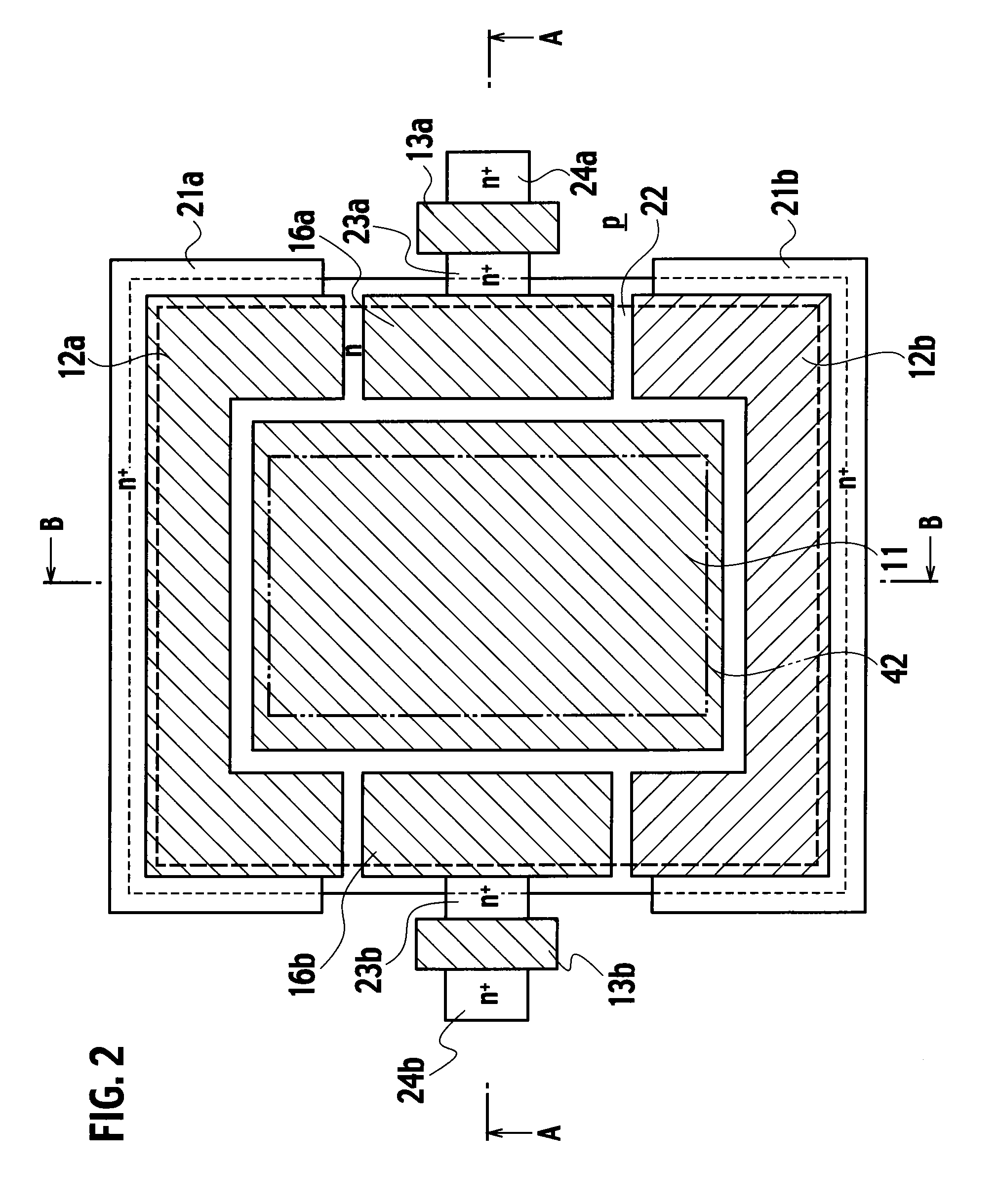
[0069]As shown in FIG. 2, in the semiconductor range-finding element according to the first embodiment, on the planar pattern, the respective central lines (whose illustrations are omitted) of the first transfer gate electrode 16a and the second transfer gate electrode 16b are aligned on the same straight line A-A in the horizontal direction (right and left direction) in FIG. 2, and the respective widths of the first transfer gate electrode 16a and the second transfer gate electrode 16b that are measured in the direction (the upper and lower direction in FIG. 2) orthogonal to the transfer direction of the signal charges are made narrower than the width of the light-receiving gate electrode 11 measured in the orthogonal direction. This structure is advantageous in that, even if the area of the light-receiving region directly under the light-receiving gate electrode 11 is increased, the perfect transfer of the signal charges through the first transfer g...

second embodiment

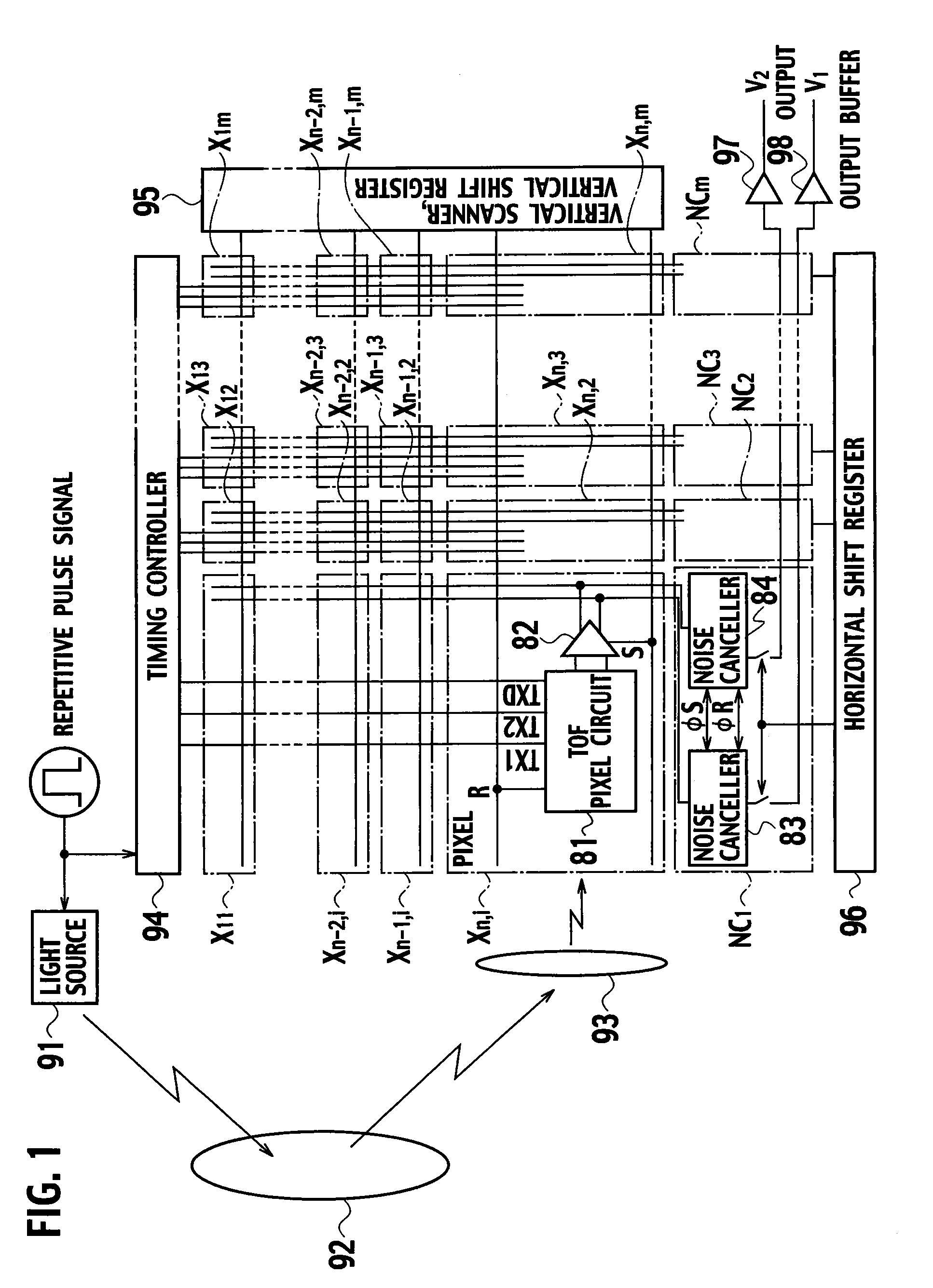
[0072]The entire configuration of a solid-state imaging device (two-dimensional image sensor) according to the second embodiment of the present invention is equivalent to the block diagram shown in FIG. 1. Thus, the overlapping or redundant description is omitted. However, the structure of the semiconductor range-finding element, which has the planar configuration shown in FIG. 12 and serves as the TOF pixel circuit 81 assigned in each of the pixels X11 to X1m, X21 to X2m, - - - , Xn1 to Xnm in the solid-state imaging device according to the second embodiment, differs from the planar configuration of the semiconductor range-finding element according to the first embodiment.

[0073]That is, the semiconductor range-finding element according to the second embodiment of the present invention has the function for reading even the component, which is caused by the background light, out to the external and canceling the background light component. Therefore, as shown in FIG. 12, a first floa...

third embodiment

[0083]The entire configuration of a solid-state imaging device (two-dimensional image sensor) according to the third embodiment of the present invention is equivalent to the block diagram shown in FIG. 1. Thus, the overlapping or redundant description is omitted. However, the structure of the semiconductor range-finding element, which has the cross-sectional structure shown in FIG. 14 and serves as the TOF pixel circuit 81 assigned in each of the pixels X11 to X1m, X21 to X2m, - - - , Xn1 to Xnm in the solid-state imaging device according to the third embodiment, differs from the cross-sectional structure of the semiconductor range-finding element according to the first embodiment, in that the semiconductor range-finding element according to the third embodiment does not contain the surface buried region 22. However, since the planar configuration is similar to the planar configuration of the semiconductor range-finding element according to the first embodiment shown in FIG. 2, the ...


PUM


Abstract

To transfer signal charges generated by a semiconductor photoelectric conversion element in opposite directions, the center line of a first transfer gate electrode and that of a second transfer gate electrodes are arranged on the same straight line, and a U-shaped first exhausting gate electrode and a second exhausting gate electrode are arranged to oppose to each other. The first exhausting gate electrode exhausts background charges generated by a background light in the charge generation region, and the second exhausting gate electrode exhausts background charges generated by the background light in the charge generation region. The background charges exhausted by the first exhausting gate electrode are received by a first exhausting drain region and the background charges exhausted by the second exhausting gate electrode are received by a first exhausting drain region.

Description

FIELD OF THE INVENTION[0001]The present invention relates to a semiconductor range-finding element and a solid-state imaging device in which semiconductor range-finding elements are arrayed one-dimensionally or two-dimensionally.DESCRIPTION OF THE RELATED ART[0002]As reported by R. Miyagawa et al., “CCD-Based Range-Finding Sensor”, IEEE Transaction on Electron Devices, October 1997, Vol. 44, No. 10, pp. 1648-1652, with a pioneering report of one-dimensional CCD range-finding sensor, which has been firstly reported in 1997, the development of time-of-flight (TOF) type range-finding sensors using time-of-flight of light and obtaining range images are advancing in many fields.[0003]However, the resolution of the currently available TOF range-finding sensor remains within about 20,000 pixels. Also, in the case of using the CCD, as the number of the pixels is increased, it becomes difficult to drive the pixels. In the hybrid method of combining CMOS manufacturing process and CCD manufact...

Claims


Application Information

Patent Timeline
IPC IPC(8): H01L31/112H01L31/06H01L31/0368G01S17/10G01S17/89
CPCG01S7/483G01S17/10G01S17/89H01L27/14689H01L27/14609H01L27/14643H01L27/14603
Inventor KAWAHITO, SHOJIHOMMA, MITSURU
Owner NAT UNIV CORP SHIZUOKA UNIV
Why Eureka
Try Eureka