Microchip

a microchip and chip technology, applied in the field of microchips, can solve the problems of inability to maximize the advantage of the microchip, and difficulty in conducting optical measurement, and achieve the effect of increasing the length of the optical path and reliable optical measuremen

Active Publication Date: 2009-05-28
HORIBA LTD
View PDF10 Cites 22 Cited by
  • Summary
  • Abstract
  • Description
  • Claims
  • Application Information

AI Technical Summary

Benefits of technology

[0010]However, avoiding such interruption of the optical path by increasing the optical path in length in the microchip's depthwise direction requires a test / analysis to be conducted with an increased amount of a specimen and an increased amount of a liquid reagent, and the microchip's advantage cannot be maximally utilized.
[0011]The present invention has been made to overcome the above disadvantage, and it contemplates a microchip including a detection portion that can prevent a substrate melted to be joined to another substrate from interrupting an optical path, and can thus ensure reliable optical measurement.

Problems solved by technology

If the substrate is raised in the fluid circuit at the detection portion, the raised substrate interrupts a portion of an optical path (i.e., a cavity provided in the detection portion to pass light therethrough for detection) and thus makes it difficult to conduct optical measurement.
However, avoiding such interruption of the optical path by increasing the optical path in length in the microchip's depthwise direction requires a test / analysis to be conducted with an increased amount of a specimen and an increased amount of a liquid reagent, and the microchip's advantage cannot be maximally utilized.

Method used


Image

  • Microchip
  • Microchip
  • Microchip

Examples


example 1

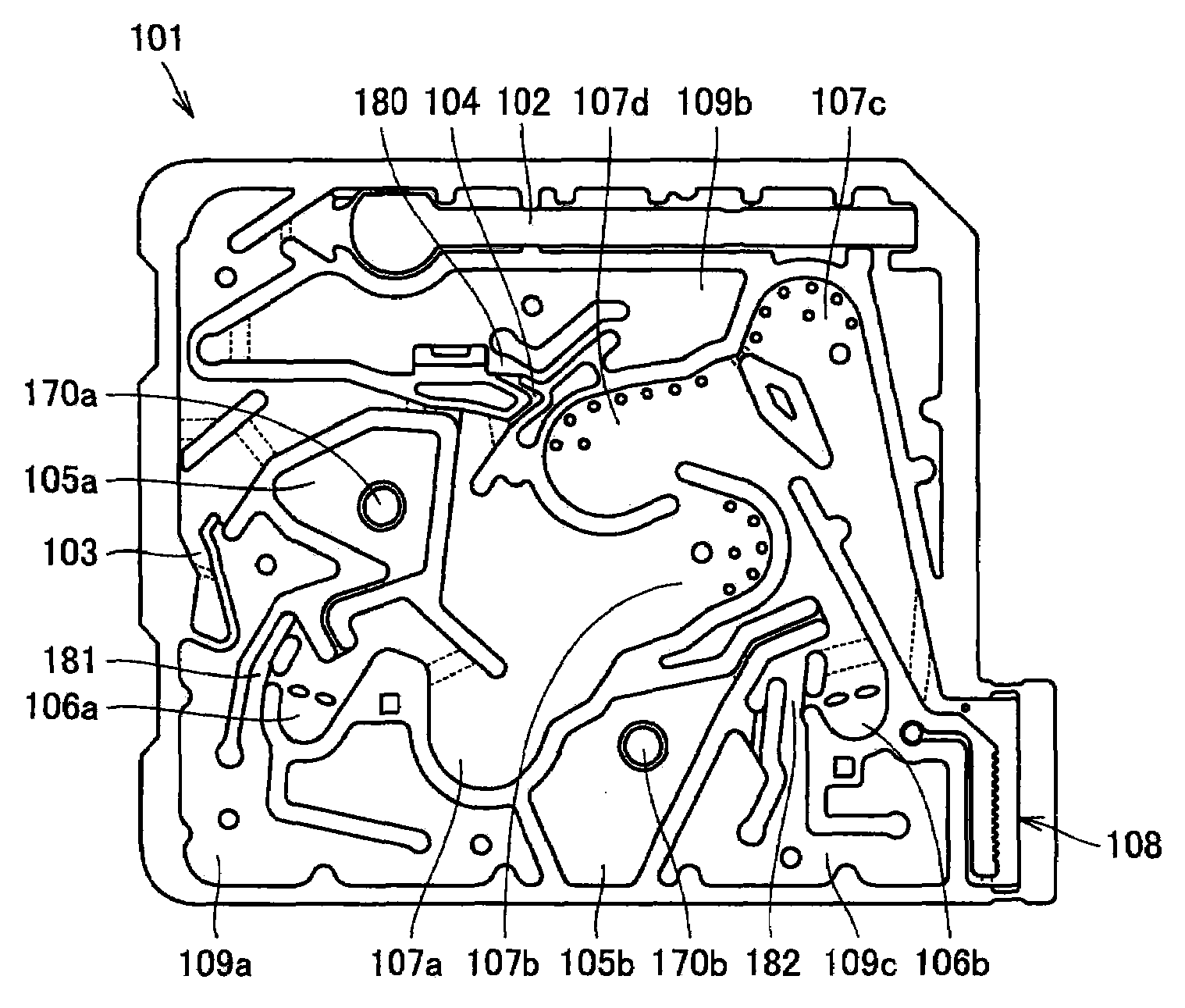
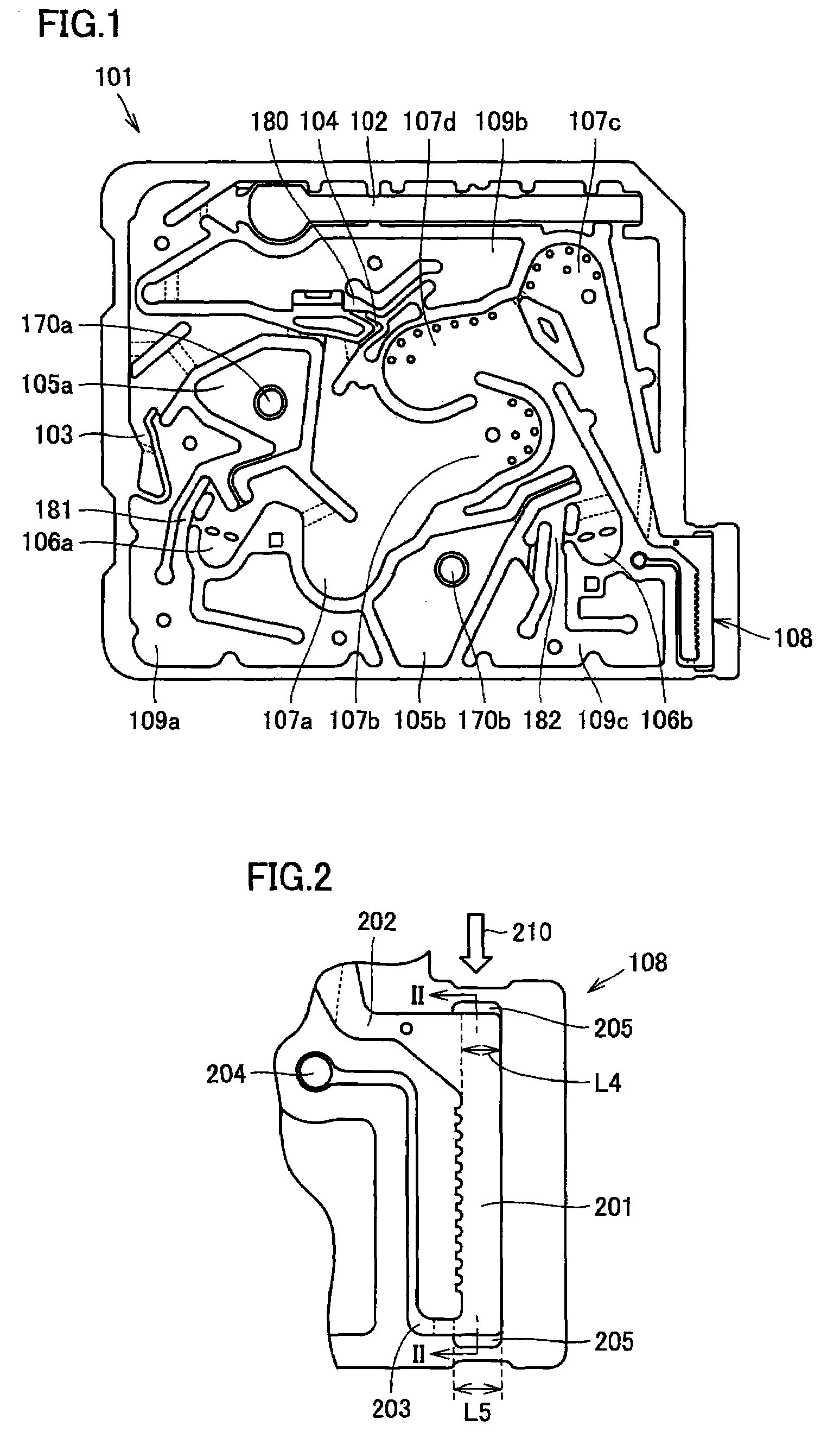
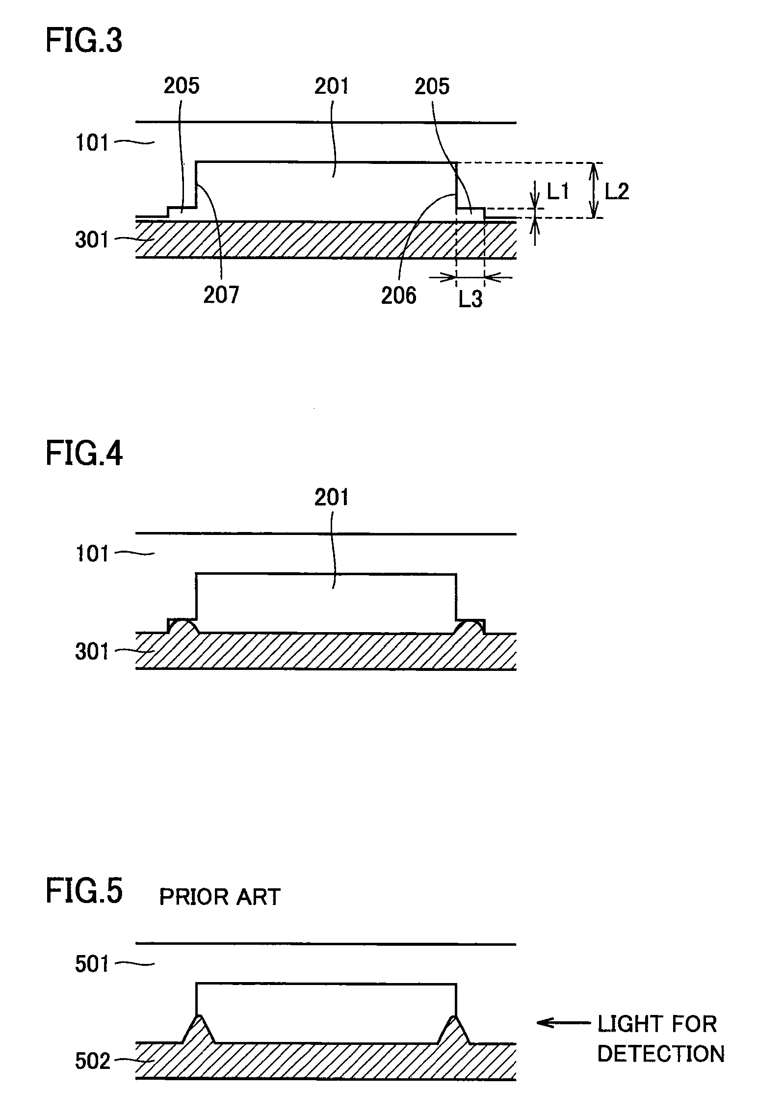
[0051]First substrate 101 having step 205, which is a transparent substrate formed of polystyrene resin and having a groove pattern as shown in FIG. 1, and second substrate 301, which is a black substrate formed of resin of polystyrene with powdery carbon mixed therewith together, as shown in FIG. 3, are prepared. Herein, step 205 has depth L1 of 0.15 mm, optical path 201 is defined by a groove having depth L2 of 1.2 mm, and step 205 has widthwise length L3 of 0.3 mm. Then, first substrate 101 and second substrate 301 are placed one on the other, and a laser is radiated to first pass through first substrate 101 to melt second substrate 301's surface to be joined to join the substrates together to obtain a microchip. Then the microchip is cut along a cross section as shown in FIG. 3. Then a CCD microscope is used to observe the cross section to measure a distance W measured from an interface of the substrates to a portion of second substrate 301 that is raised most. Such measurement ...


PUM

PropertyMeasurementUnit
depthaaaaaaaaaa
depthaaaaaaaaaa
depthaaaaaaaaaa

Abstract

There is provided a microchip that is formed of a first substrate having a surface with a groove and a second substrate joined together and has a fluid circuit in the form of a cavity defined by the groove and a surface of the second substrate closer to the first substrate. The fluid circuit at least includes a detection portion having an optical path for transmitting light. The microchip includes at least one of a step defined by a groove formed in contact with at least one side surface of a groove of the first substrate that defines the optical path and a recess provided in the second substrate at a position opposite to the step.

Description

BACKGROUND OF THE INVENTION[0001]1. Field of the Invention[0002]The present invention relates generally to microchips useful as a micro total analysis system (μ-TAS) or the like suitably used for biochemical test of DNA, protein, cell, immunity, blood and the like, chemical synthesis and environmental analysis and the like, and particularly to microchips having a detection portion for optical measurement.[0003]2. Description of the Background Art[0004]In recent years in the fields of medical care, health, food, medicine development and the like it has been increasingly important to sense, detect or assay deoxyribo nucleic acid (DNA), enzymes, antigen, antibody, protein, viruses, cells and other similar biological substances and chemical substances, and there have been proposed a variety of biochips and micro chemical chips that can measure such substances conveniently. (Hereinafter such chips will be referred to as a “microchip” collectively.)[0005]The microchip allows a series of t...

Claims


Application Information

Patent Timeline
Patent Type & Authority Applications(United States)
IPC IPC(8): G01N33/48
CPCG01N33/4915
Inventor KAGEYAMA, YASUHISAMORI, TOSHIHIRO
Owner HORIBA LTD
Why Eureka
Try Eureka