Thin film solar cell and method for manufacturing same

a solar cell and film technology, applied in the field of thin film solar cells, can solve the problems of insufficient suppression of reflection by the substrate, limited design, and peeling of the layer, and achieve the effects of improving the light confinement effect, improving the optical path length of incident light, and improving the characteristics of solar cells

Inactive Publication Date: 2014-05-08
KANEKA CORP
View PDF8 Cites 9 Cited by
  • Summary
  • Abstract
  • Description
  • Claims
  • Application Information

AI Technical Summary

Benefits of technology

[0027]According to the present invention, since a transparent substrate has a transparent undercoat layer and an insulating irregularity layer, reflection of light by the transparent substrate is suppressed, and the optical path length of incident light is increased due to light scattering, so that an improved light confinement effect is exhibited. Therefore, a thin film solar cell of the present invention may capture a large amount of light in a photoelectric conversion unit, and resultantly solar cell characteristics may be improved.

Problems solved by technology

However, when a transparent conductive oxide layer is formed directly on a smooth base as in Patent Document 1, possibility of design is limited because the crystal structure of the transparent conductive oxide influences the irregularity shape.
In Patent Document 2, however, suppression of reflection by a substrate is not sufficient, and there is a room for improvement.
When an irregularity layer is formed by nano-imprint on a smooth base such as a glass plate as in Patent Document 2, adhesion between the base and the irregularity layer is not sufficient, and therefore peeling of the layer may occur.
When a transparent substrate has an irregularity shape, laser processing accuracy and its reliability tend to be deteriorated because laser light is scattered at the irregular interface of the substrate at the time of patterning a thin film solar cell to be integrated.
This method has the problem that the process for formation of irregularities is complicated, and it is thus difficult to improve production efficiency of an integrated thin film solar cell.

Method used


Image

  • Thin film solar cell and method for manufacturing same
  • Thin film solar cell and method for manufacturing same
  • Thin film solar cell and method for manufacturing same

Examples


example 1

Formation of Undercoat Layer

[0155]An alkali-free glass plate (trade name: OA-10; manufactured by Nippon Electric Glass Co., Ltd.; thickness: 0.7 mm) was used as a glass base, and a transparent undercoat layer was formed on the glass plate.

[0156]11.90 g of an oligomer of tetraethoxysilane (polymerization degree n: 4 to 6) as a binder, and 24.38 g of an aqueous dispersion (solid content: 40%) of a silica fine particle component having an average particle size of 90 nm as fine particles were sequentially added to a mixed liquid of 24.38 g of water, 58.71 g of isopropyl alcohol and 1.14 g of 35% hydrochloric acid. The mixture was stirred / mixed at room temperature for 4 hours. Thereafter, 529.50 g of isopropanol was added as a diluent solvent, and the mixture was stirred to prepare a fine particle-containing coating solution.

[0157]A coating was performed by a dip coating method of dipping the glass base in the coating solution and drawing up the glass base at a speed of 0.1 m / minute. Dip...

example 2

Formation of Undercoat Layer

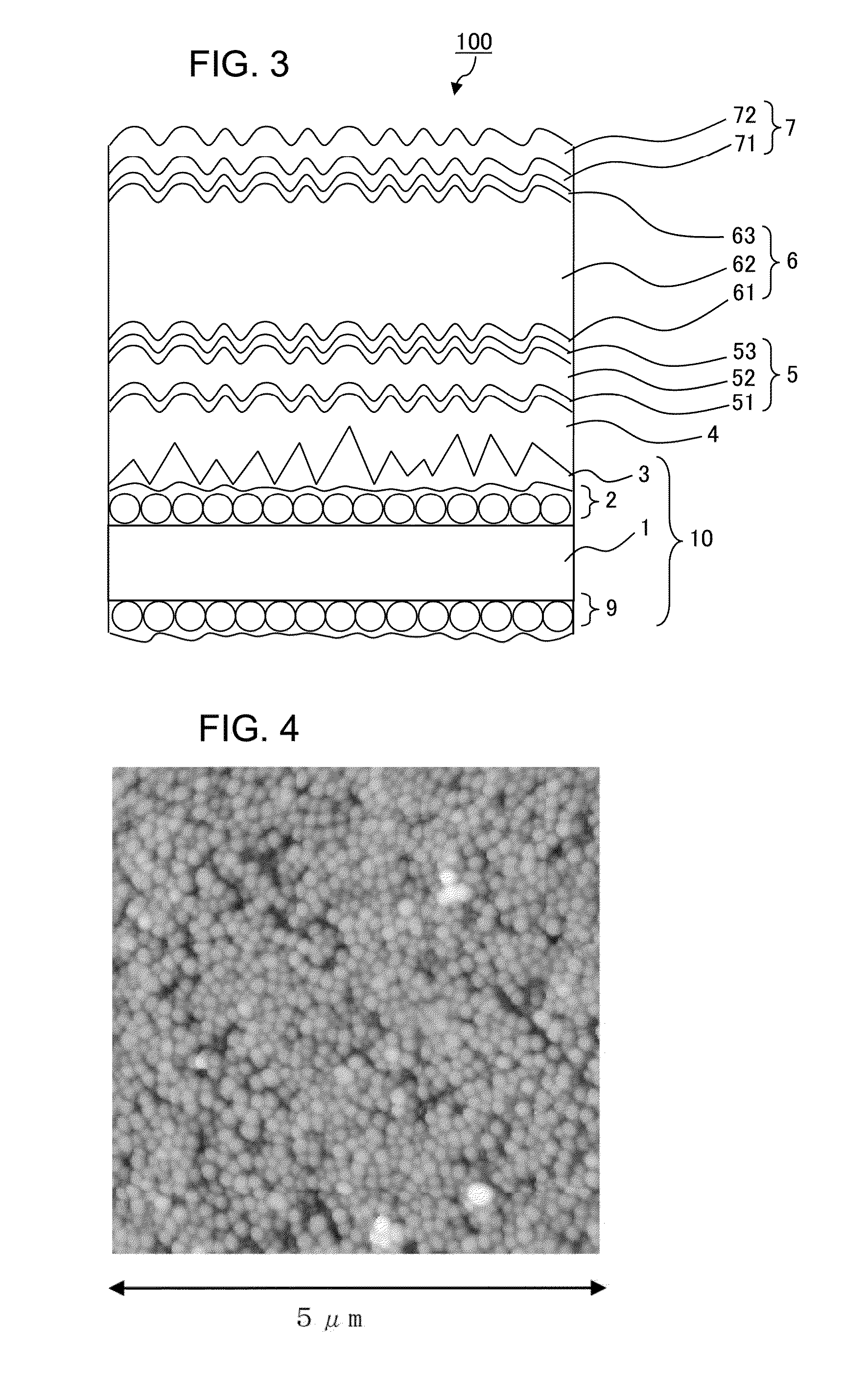
[0169]A transparent undercoat layer was formed on a glass base in the same manner as in example 1. In the obtained substrate with a transparent undercoat layer, the area coverage with silica fine particles was 90%, and a dense irregularity shape was observed.

[0170][Preparation of Matrix]

[0171]First, an oxide film (silicon oxide film) was formed on the surface of a single-crystal silicon wafer by thermal oxidation. A resist (photosensitive protective film) was applied by spin coating to the entire surface of the single-crystal on which the oxide film is formed. Next, using a photomask having circular openings with a diameter of 700 μm at pitches of 1000 μm, UV light with a wavelength of 365 nm was applied to expose the silicon wafer at the openings. The UV light-exposed wafer was dipped in a developer to develop a pattern of the photomask, so that a resist film was selectively formed on the wafer surface. Next, etching was performed using hydrofluoric acid...

reference example 1

[0196]In Reference Example 1, the amount of fine particles in a fine particle-containing coating solution for forming a transparent undercoat layer was increased as compared to Example 1. Otherwise in the same manner as in Example 1, a transparent undercoat layer was formed on a glass base. The arithmetic mean roughness of the surface of the transparent undercoat layer was 19 nm, and the coverage with fine particles was 95%. An insulating irregularity layer was formed on the transparent undercoat layer in the same manner as in Example 1.


PUM


Abstract

The invention relates to a thin film solar cell including a transparent substrate, a transparent electrode layer, at least one photoelectric conversion unit, and a back electrode layer in this order from the light incident side. The transparent substrate includes a transparent base, a transparent undercoat layer having fine particles and a binder, and an insulating irregularity layer in this order from the light incident side. Consequently, light reflection by the transparent substrate is suppressed and optical path length of the incident light is increased due to light diffusion, so that improved optical confinement effect can be achieved.

Description

TECHNICAL FIELD[0001]The invention relates to a thin film solar cell having high light-capturing efficiency and a method for manufacturing the same.BACKGROUND ART[0002]A thin film solar cell includes a transparent electrode layer, a photoelectric conversion unit formed of a semiconductor silicon or the like, and a back electrode layer on a transparent substrate. The thin film solar cell is modularized by patterning each layer by laser light irradiation to be divided into a plurality of unit cells, and connecting the unit cells in series or in parallel to be integrated.[0003]One of the measures for improving photoelectric conversion efficiency of the thin film solar cell is “improvement of light confinement efficiency”. Light confinement utilizes the following phenomenon: the optical path length of incident light from the transparent substrate side is increased due to light scattering in a transparent electrode layer and a photoelectric conversion layer and refraction of light at the...

Claims


Application Information

Patent Timeline
Patent Type & Authority Applications(United States)
IPC IPC(8): H01L31/0236H01L31/18
CPCH01L31/1884H01L31/02366H01L31/022466H01L31/0463H01L31/02168H01L31/0392H01L31/046H01L31/0465H01L31/03923H01L31/03925Y02E10/541H01L31/022483Y02P70/50
Inventor INAKI, OSAMUMEGURO, TOMOMIKOIZUMI, GENSUKENAKANISHI, NAOAKIYAMAMOTO, KENJI
Owner KANEKA CORP
Why Eureka
Try Eureka