Method of plasma treatment using amplitude-modulated RF power

Active Publication Date: 2009-05-28
ASM JAPAN
View PDF7 Cites 341 Cited by
  • Summary
  • Abstract
  • Description
  • Claims
  • Application Information

AI Technical Summary

Benefits of technology

[0009]In at least one embodiment of the present invention, only a gas that does not form film is supplied and a high-frequency power that has been amplitude-modulated is applied to

Problems solved by technology

This substrate voltage remains in the substrate after the film forming process has completed, and may sometimes cause the substrate to be attracted to the substrate processing base, in which case a problem will occur in the subsequent process of transferring the substrate.
However, the aforementioned method presents problems in that it cannot lower the substrate voltage sufficiently i

Method used


Image

  • Method of plasma treatment using amplitude-modulated RF power
  • Method of plasma treatment using amplitude-modulated RF power
  • Method of plasma treatment using amplitude-modulated RF power

Examples


example 1

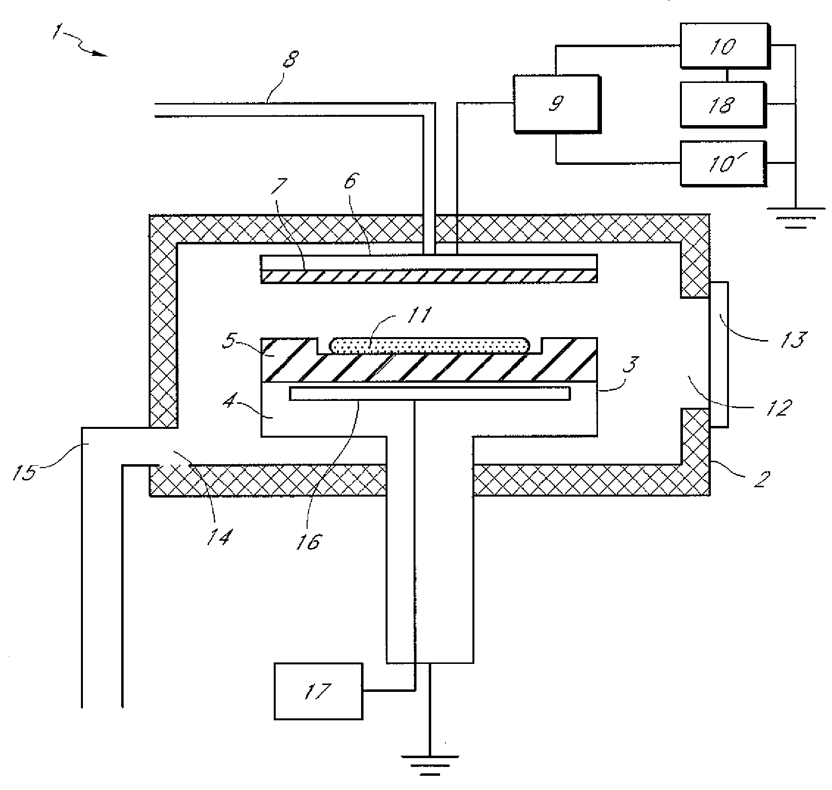
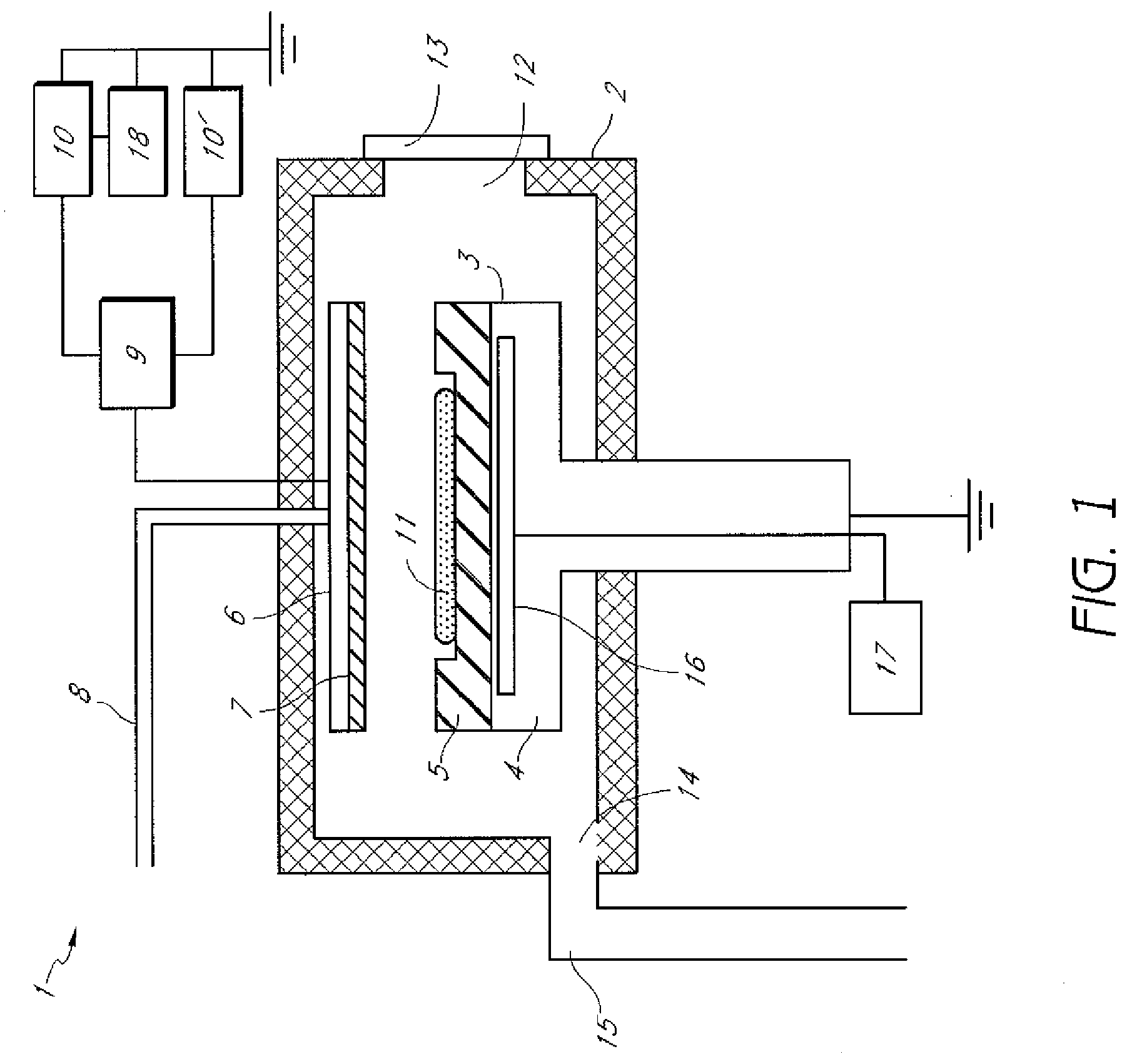
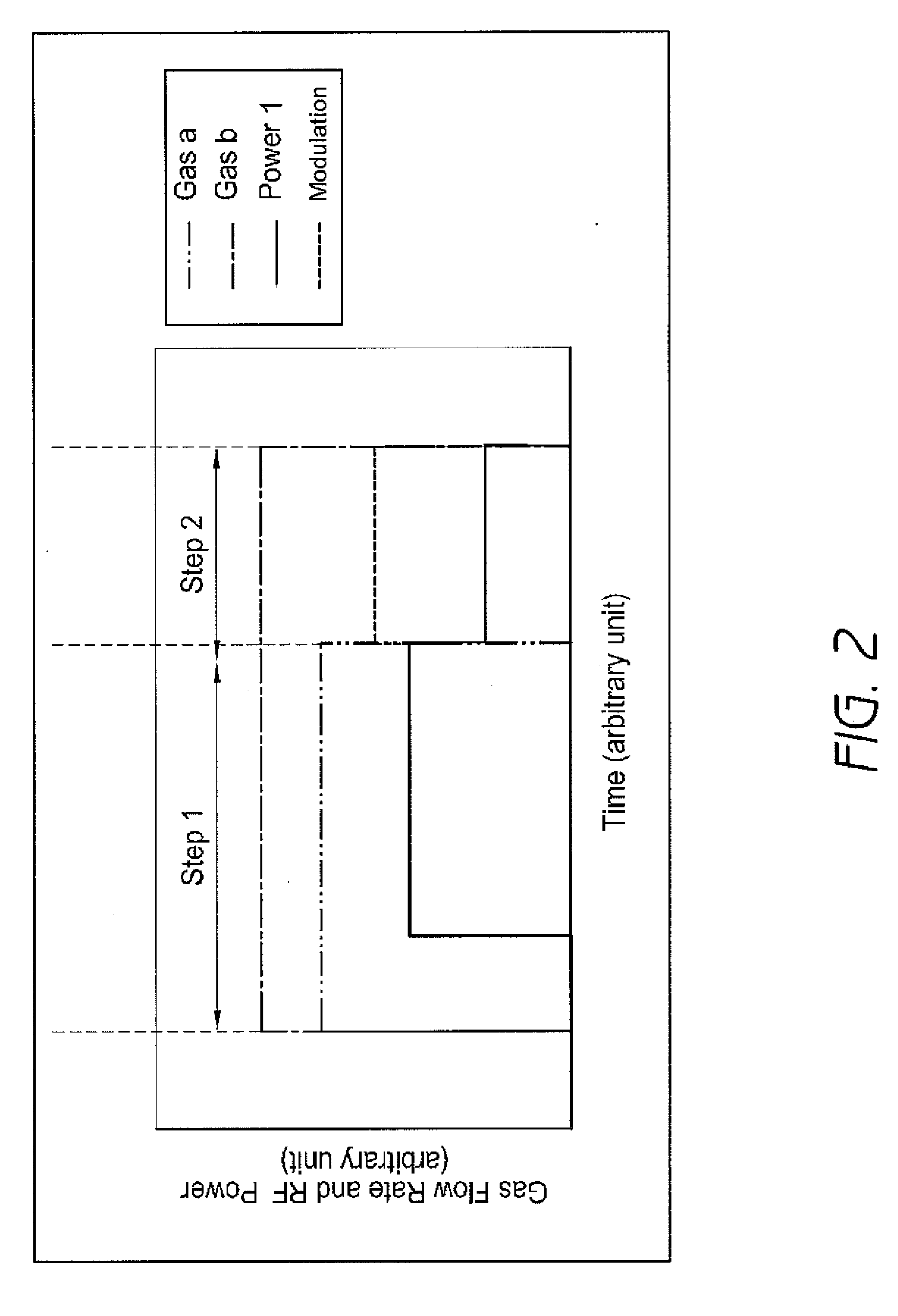
[0062]The best mode for carrying out the present invention is explained below by referring to FIG. 2.

[0063]Step 1 indicates a film forming process or film termination treatment process, while step 2 indicates a process of removing electric charges by means of modulation. In the figure, gas a indicates a reaction gas, while gas b indicates an additive gas. Both the vertical and horizontal axes represent arbitrary units, and changes along each axis are not scaled. Modulation is expressed by an on / off state.

[0064]The reaction gas is stopped and only the additive gas is supplied after the film forming process or film termination process has completed, and if RF power of 430 kHz is used, then application of the 430-kHz RF power is stopped and RF power of 13.56 MHz alone, which has been adjusted to 20 W, is applied for approx. 3 seconds at a constant electric power to cause discharge. At this time, the RF power is amplitude-modulated at a modulation frequency of 5 kHz and amplitude modula...

example 2

[0066]Another example of the present invention is explained below by referring to FIG. 3.

[0067]Step 1 indicates a film forming process or film termination treatment process, while step 2 indicates a process of removing electric charges by means of modulation. In the figure, gas a indicates a reaction gas, while gas b indicates an additive gas.

[0068]The reaction gas is stopped and only the additive gas is supplied after the film forming process or film termination process has completed, and if RF power of 430 kHz is used, then application of the 430-kHz RF power is stopped and RF power of 13.56 MHz alone is applied for approx. 3 seconds.

[0069]At this time, the RF power is amplitude-modulated at a modulation frequency of 5 kHz and amplitude modulation ratio of 1, and the electric power is gradually decreased from the same level used during the film forming process in such a way that the electric power becomes 0 W when the process ends (the electric power is decreased linearly).

[0070]I...

example 3

[0071]Although the electric power is gradually decreased in Example 2 given above, the voltage may be lowered in several steps as shown in FIG. 4, or the rate at which the voltage is lowered may be changed in each of these steps. It is also possible to combine Examples 1, 2 and / or 3.


PUM

PropertyMeasurementUnit
Timeaaaaaaaaaa
Timeaaaaaaaaaa
Poweraaaaaaaaaa

Abstract

A method for processing a substrate by plasma CVD includes: (i) forming a film on a substrate placed on a susceptor by applying RF power between the susceptor and a shower plate in the presence of a film-forming gas in a reactor; and (ii) upon completion of step (i), without unloading the substrate, applying amplitude-modulated RF power between the susceptor and the shower plate in the absence of a film-forming gas but in the presence of a non-film-forming gas to reduce a floating potential of the substrate.

Description

BACKGROUND OF THE INVENTION[0001]1. Field of the Invention[0002]The present invention generally relates to semiconductor processing in a plasma treatment apparatus, particularly to a method of reducing a floating potential of a substrate upon film formation.[0003]2. Description of the Related Art[0004]In capacity-coupled plasma CVD, a floating voltage is generated on a substrate placed on a substrate processing base while film is being formed. This substrate voltage remains in the substrate after the film forming process has completed, and may sometimes cause the substrate to be attracted to the substrate processing base, in which case a problem will occur in the subsequent process of transferring the substrate.[0005]The sticking force that applies between the wafer and electrode is expressed by the formula below:F=ɛ0ɛrSVw22d2[0006]Here, F (N) indicates the sticking force, ε0 (F / m) indicates the dielectric constant in vacuum, εr indicates the specific dielectric constant of anodic o...

Claims


Application Information

Patent Timeline
IPC IPC(8): H05H1/24
CPCC23C16/505H01J37/32146H01J37/32091
Inventor FUKASAWA, YASUSHISHUTO, MITSUTOSHISUZUKI, YASUAKI
Owner ASM JAPAN
Why Eureka
Try Eureka