Chip Handler with a Buffer Traveling between Roaming Areas for Two Non-Colliding Robotic Arms

a robot arm and chip handler technology, applied in the field of robot semiconductor test systems, can solve the problems of high testing cost, high cost of high-speed electronic test equipment, and high cost of memory industry

Active Publication Date: 2009-05-28
KINGSTON DIGITAL CO LTD
View PDF20 Cites 21 Cited by
  • Summary
  • Abstract
  • Description
  • Claims
  • Application Information

AI Technical Summary

Problems solved by technology

The memory industry is quite cost sensitive.
Testing costs are significant, especially for higher-density chips and modules.
Specialized, high-speed electronic test equipment is expensive, and the greater number of memory cells on high-speed memory chips increases the time spent on the tester, increasing test costs.
However, simply increasing the number of test sockets may increase delays as robotic arms must travel longer distances.
Adding more robotic arms can result in collisions among robotic arms, or in delays while one robotic arm waits for another robotic arm to get out of the way.

Method used


Image

  • Chip Handler with a Buffer Traveling between Roaming Areas for Two Non-Colliding Robotic Arms
  • Chip Handler with a Buffer Traveling between Roaming Areas for Two Non-Colliding Robotic Arms
  • Chip Handler with a Buffer Traveling between Roaming Areas for Two Non-Colliding Robotic Arms

Examples


Embodiment Construction

[0014]The present invention relates to an improvement in multi-robotic-arm chip testers. The following description is presented to enable one of ordinary skill in the art to make and use the invention as provided in the context of a particular application and its requirements. Various modifications to the preferred embodiment will be apparent to those with skill in the art, and the general principles defined herein may be applied to other embodiments. Therefore, the present invention is not intended to be limited to the particular embodiments shown and described, but is to be accorded the widest scope consistent with the principles and novel features herein disclosed.

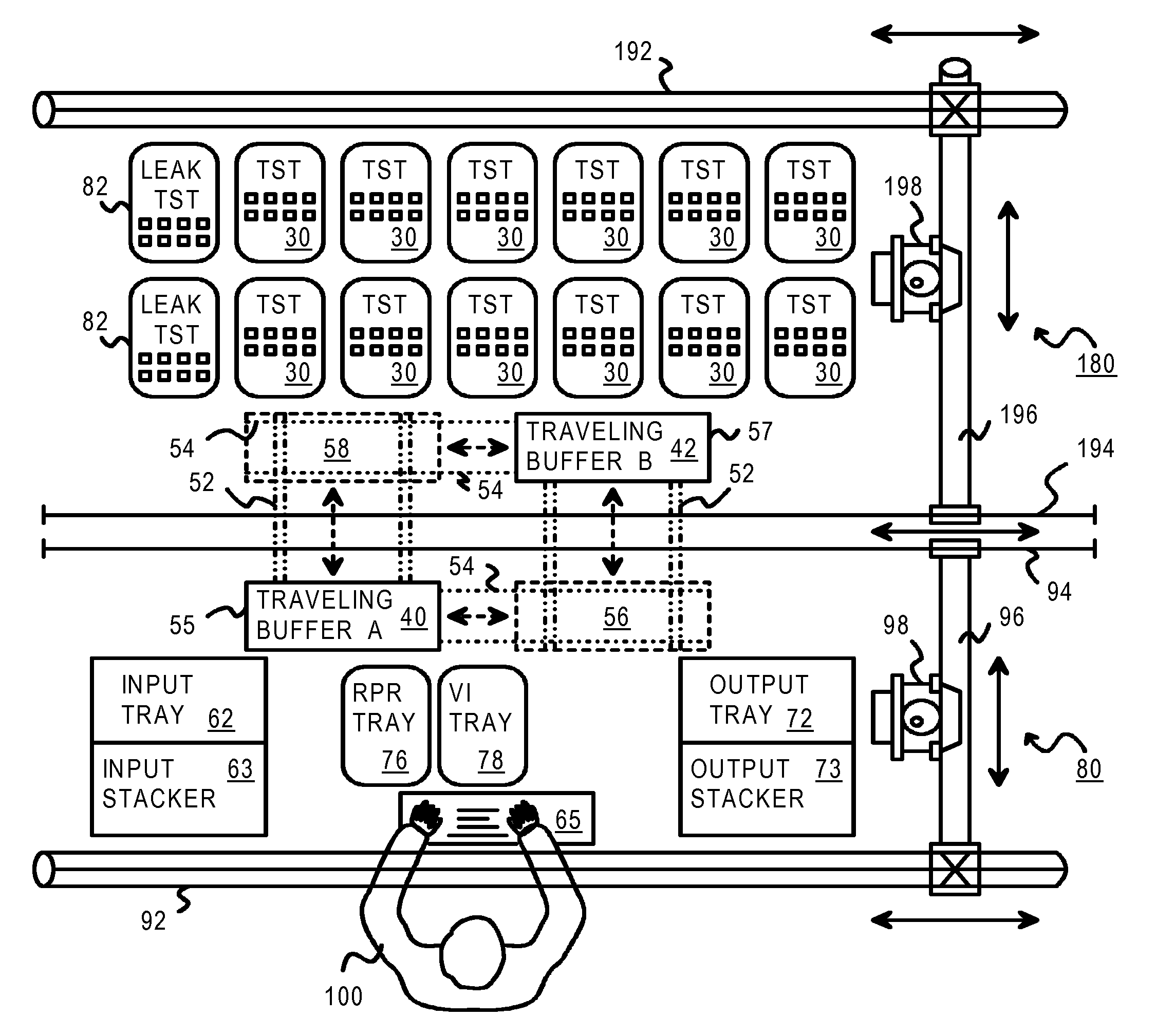
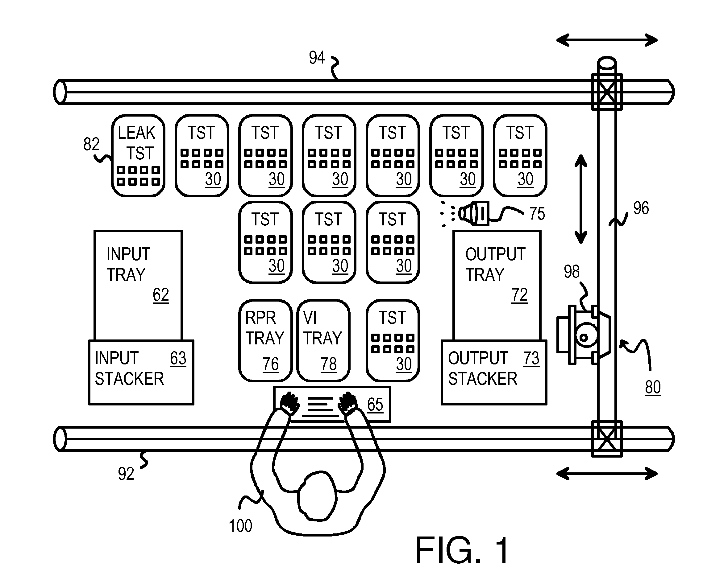
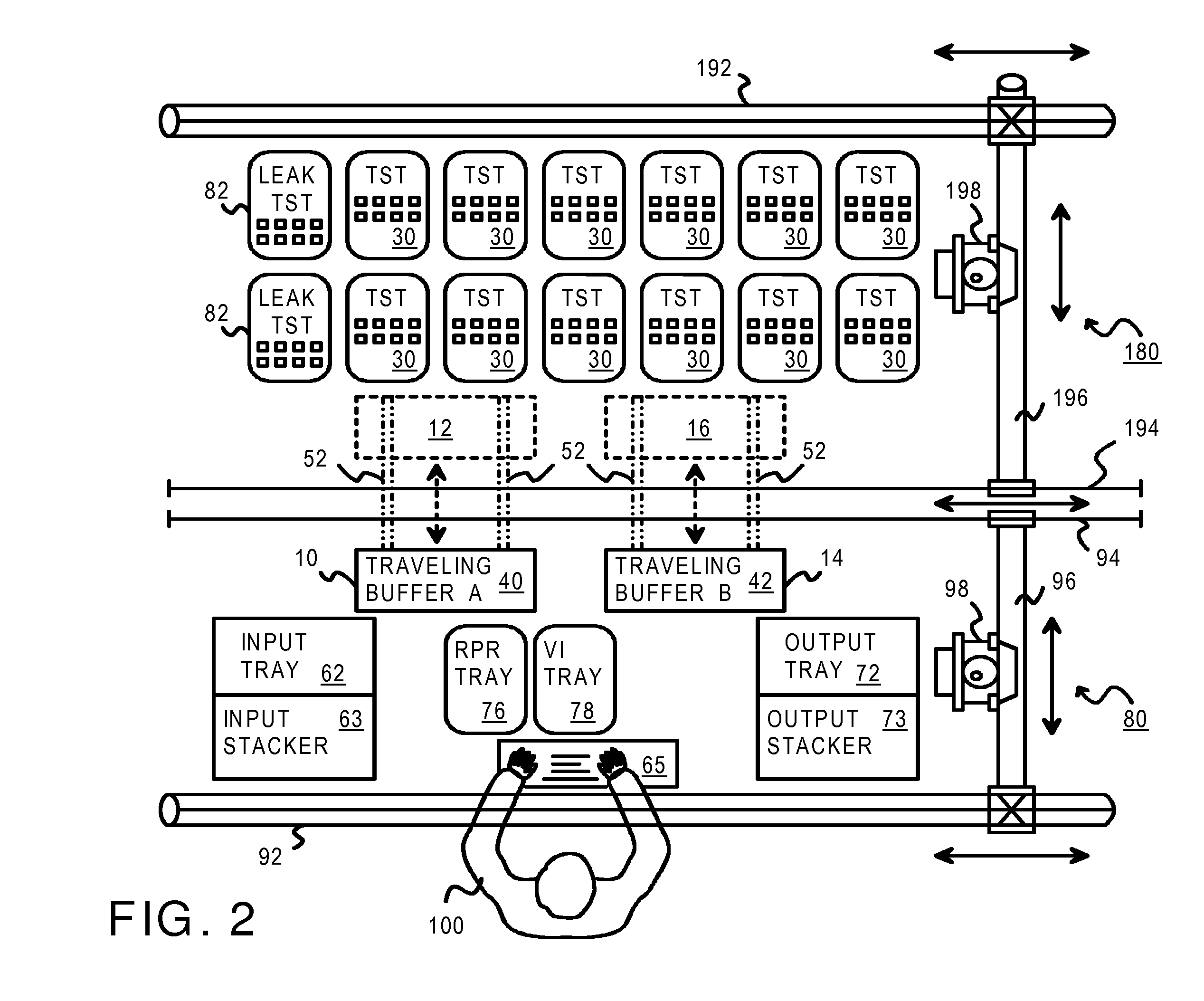
[0015]FIG. 1 is an overhead diagram looking down on a multi-board test station with overhead rails for an x-y-z robotic handler. Operator 100 can sit in front of the test station, controlling operation with a touch-screen or keyboard. Trays of untested memory IC chips such as DRAM chips can include a barcode that is sca...


PUM


Abstract

Two robotic arms roam in separate, non-overlapping areas of a test station, avoiding collisions. A traveling buffer moves along x-tracks between a front position and a back position. In the front position, a first robotic arm loads IC chips from an input tray or stacker into buffer cavities in the traveling buffer. The traveling buffer then moves along the x-tracks to the back position, where a second robotic arm moves chips from the traveling buffer to test boards for testing. After testing, the second robotic arm moves chips to a second traveling buffer, which then moves along tracks to a front position for unloading by the first robotic arm. Two traveling buffers may move on the same tracks in a loop. The buffer cavities in the traveling buffer move on internal tracks to expand and contract spacing and pitch between the front and back positions to match test-board pitch.

Description

RELATED APPLICATION[0001]This application may be related to U.S. Pat. No. 6,415,397 for “Automated Multi-PC-Motherboard Memory-Module Test System with Robotic Handler and In-Transit Visual Inspection” and U.S. Ser. No. 10 / 249,841 for “Robotic Memory-Module Tester Using Adapter Cards for Vertically Mounting PC Motherboards”, having a common assignee and at least one inventor in common, but presenting patentably distinct claims.FIELD OF THE INVENTION[0002]This invention relates to robotic semiconductor test systems, and more particularly to movable chip-tray buffers for use with multiple robotic arms.BACKGROUND OF THE INVENTION[0003]Semiconductor integrated circuit (IC) chips are widely used in consumer electronics, telecommunications, and computer systems such as personal computers (PCs). A wide variety of semiconductor chips are made, including analog, system-on-a-chip, microprocessor, controllers, and memory. Perhaps the most widely made are dynamic random-access memory (DRAM) chip...

Claims


Application Information

Patent Timeline
Patent Type & Authority Applications(United States)
IPC IPC(8): G06F19/00
CPCB25J9/16G05B19/4182B25J9/1666Y02P90/02
Inventor CO, RAMON S.LAI, TAT LEUNGLEONG, CALVIN G.
Owner KINGSTON DIGITAL CO LTD
Why Eureka
Try Eureka