Layout design method of semiconductor integrated circuit by using soft macro

a semiconductor integrated circuit and design method technology, applied in the field of semiconductor integrated circuit layout design method, can solve the problems of increasing design man-hour, affecting chip wireability, and affecting chip wireability, so as to reduce the number of layout repetitions for timing convergence, reduce the effect of design man-hour and suppress the increase of chip area

Inactive Publication Date: 2009-06-04
RENESAS ELECTRONICS CORP
View PDF1 Cites 4 Cited by
  • Summary
  • Abstract
  • Description
  • Claims
  • Application Information

AI Technical Summary

Benefits of technology

The patent text describes a method for designing a layout of a semiconductor integrated circuit in an integrated circuit chip. The method involves reading a netlist and a soft macro, which includes information about the relative positions of cells and wiring lines in the circuit. The layout design method then determines the coordinates of the cells and wiring lines in the chip, and specifies the arrangement position of cells that have undetermined positions. This helps to reduce the area of the chip and minimize the number of layout repetitions for timing convergence and design man-hour. The patent also describes a computer-readable medium that records a data structure for automated layout design of the semiconductor integrated circuit.

Problems solved by technology

Also, wiring routes of wiring lines not included in the macro cannot be determined to extend through the area occupied by the macro.
In such a case, in order to attain timing convergence for the critical path in the macro, a designer should repeatedly perform manual arrangement and wiring to carry out the layout, and consequently there arises a problem of an increase in design man-hour.
For this reason, wireability at a chip level may deteriorate.
Further, wiring delay caused by the net bypassing the hard macro portion 102 may be increased and wiring congestion may appear.

Method used


Image

  • Layout design method of semiconductor integrated circuit by using soft macro
  • Layout design method of semiconductor integrated circuit by using soft macro
  • Layout design method of semiconductor integrated circuit by using soft macro

Examples


first embodiment

[0043]According to a first embodiment of the present invention, layout of a semiconductor integrated circuit to be designed is determined with the use of a computer provided with a design support tool. The computer operates according to a procedure instructed by a computer program stored therein to thereby function as a design support tool.

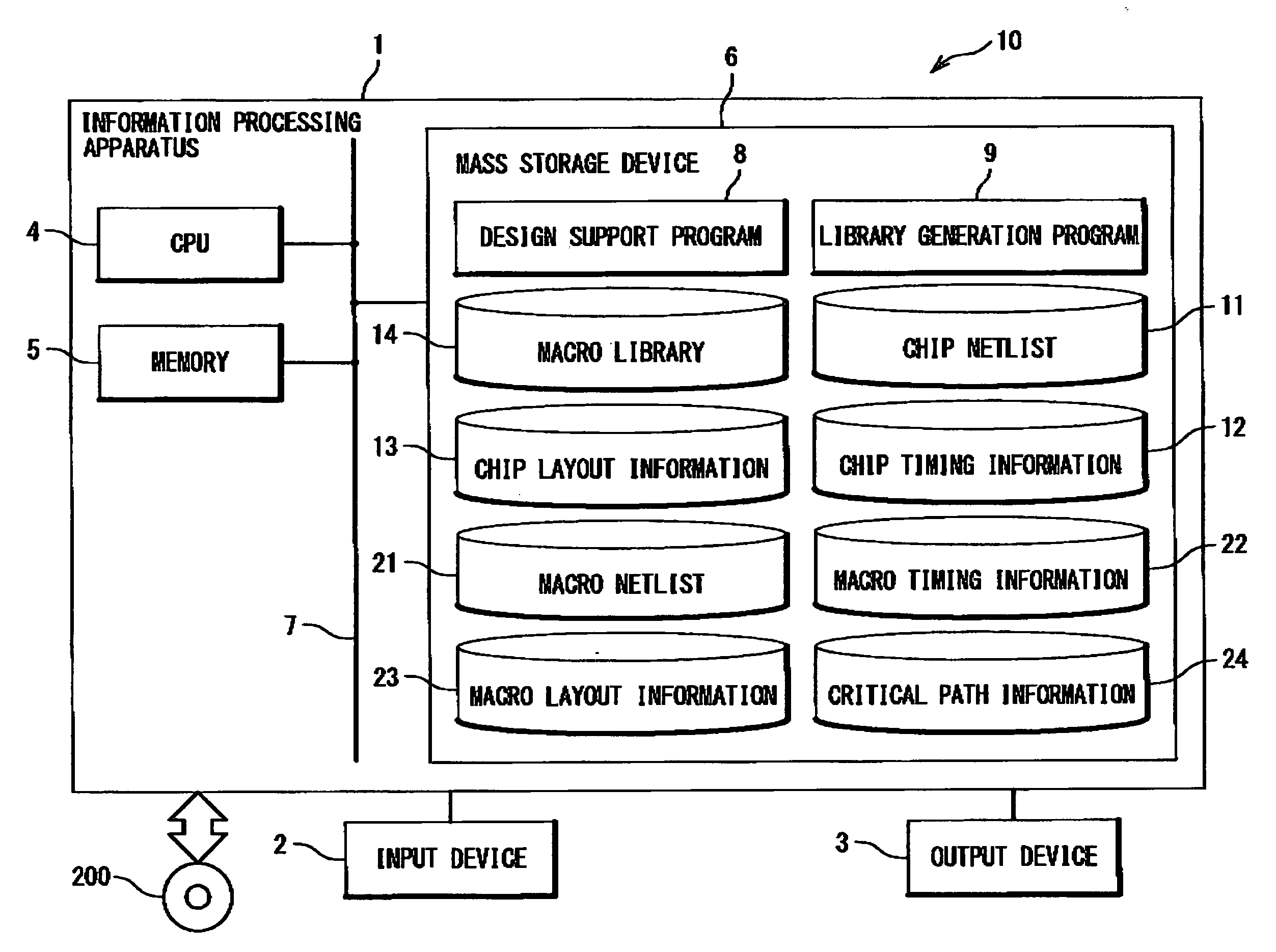
[0044]FIG. 4 is a block diagram of a semiconductor device design support system 10 according to the present embodiment. The semiconductor device design support system 10 includes an information processing apparatus 1, an input device 2, and an output device 3. The information processing apparatus 1 is a device (computer) which is caused by programs to execute a layout design method of semiconductor integrated circuit by using soft macro and a method for generating a soft macro library. The information processing apparatus 1 is provided with five basic functions, i.e., input, storage, calculation, control, and output. The input device 2 is a man-ma...

second embodiment

[0073]A second embodiment of the present invention is described below referring to the drawings. FIG. 12 is a plan view exemplifying a configuration of a macro cell 41 according to the second embodiment. Configuration and operation of a semiconductor device design support system 10 according to the second embodiment are same as those of the system 10 according to the first embodiment, but may be modified as necessary to suit the macro cell 14 according to the second embodiment. In the following descriptions, to facilitate understanding of configuration and operation according to the present embodiment, a duplicate description of a same portion as that of the above-described embodiment is omitted.

[0074]Referring to FIG. 12, the macro cell 41 according to the second embodiment includes a wiring prohibited area 54. The wiring prohibited area 54 is provided around functional blocks 43, primitive cells 44, and wiring lines 45 in relative arrangement position determined area 42, and confi...

third embodiment

[0076]A third embodiment of the present invention is described below referring to the drawings. FIG. 14 is a plan view exemplifying a configuration of a macro cell 41 according to the third embodiment. Configuration and operation of a semiconductor device design support system 10 according to the third embodiment are same as those of the system 10 according to the first embodiment, but may be modified as necessary to suit the macro cell 14 according to the third embodiment. In the following descriptions, to facilitate understanding of configuration and operation according to the present embodiment, a duplicate description of the same portion as those of the above-described embodiments is omitted. Referring to FIG. 14, the macro cell 41 according to the third embodiment includes shielding lines 55. The shielding lines 55 suppress wiring lines 45 in relative arrangement position determined area 42 from influencing other net wiring lines.

[0077]FIG. 15 exemplifies a data structure of a ...


PUM


Abstract

A layout design method of a semiconductor integrated circuit to be formed in an integrated circuit (IC) chip is provided. The layout design method includes reading a netlist and a soft macro. The soft macro includes: relative position information describing relative positions of a plurality of relative arrangement position determined cells; and wiring information describing positions of arrangement position determined wiring lines arranged in corresponding to the plurality of relative position determined cells. The layout design method further includes: determining coordinates of the plurality of relative arrangement position determined cells in the IC chip based on the relative position information; determining wiring routes of the arrangement position determined wiring lines in the IC chip based on the coordinates and the wiring information; and determining an arrangement position of an arrangement position undetermined cell in the IC chip. The arrangement position undetermined cell is a cell of which arrangement position in the IC chip is undetermined in advance.

Description

INCORPORATION BY REFERENCE[0001]This application is based upon and claims the benefit of priority from Japanese patent application No. 2007-308994, filed on Nov. 29, 2007, the disclosure of which is incorporated herein in its entirely by reference.BACKGROUND OF THE INVENTION[0002]1. Field of the Invention[0003]The present invention relates to a semiconductor integrated circuit, and more particularly, to a layout design method of semiconductor integrated circuit by using soft macro, a data structure of the soft macro, and a method for generating a soft macro library.[0004]2. Description of Related Art[0005]There is known a design method of a semiconductor integrated circuit by using soft or hard macro which describes a macro (functional module) as a function of the semiconductor integrated circuit.[0006]The hard macro describes fixed arrangements of a plurality of primitive cells included in the macro and fixed wiring routes between the primitive cells. Information on the shape, inpu...

Claims


Application Information

Patent Timeline
Patent Type & Authority Applications(United States)
IPC IPC(8): G06F17/50
CPCG06F17/5077G06F30/394
Inventor ANDOU, TETSUO
Owner RENESAS ELECTRONICS CORP
Why Eureka
Try Eureka