Method for manufacturing n-type and p-type chalcogenide material, doped homojunction chalcogenide thin film transistor and method of fabricating the same

a technology of chalcogenide thin film transistor and homojunction chalcogenide, which is applied in the direction of transistors, electrical devices, semiconductor devices, etc., can solve the problems of high-cost silicon substrate, complicated structure of photo thin film transistor actually fabricated through a cmos process, etc., and achieve low cost and great mobility

Inactive Publication Date: 2009-06-11
ELECTRONICS & TELECOMM RES INST
View PDF8 Cites 19 Cited by
  • Summary
  • Abstract
  • Description
  • Claims
  • Application Information

AI Technical Summary

Benefits of technology

[0046]Also, the thin film transistor according to the present invention can be operated on a plastic substrate as well as can be fabricated using a low-temperature process, without ion-implantation, having an advantage that it...

Problems solved by technology

A structure of a photo thin film transistor actually fabricated through a CMOS process is more complicated.
In particular, the thin film transistor fa...

Method used


Image

  • Method for manufacturing n-type and p-type chalcogenide material, doped homojunction chalcogenide thin film transistor and method of fabricating the same
  • Method for manufacturing n-type and p-type chalcogenide material, doped homojunction chalcogenide thin film transistor and method of fabricating the same
  • Method for manufacturing n-type and p-type chalcogenide material, doped homojunction chalcogenide thin film transistor and method of fabricating the same

Examples


Embodiment Construction

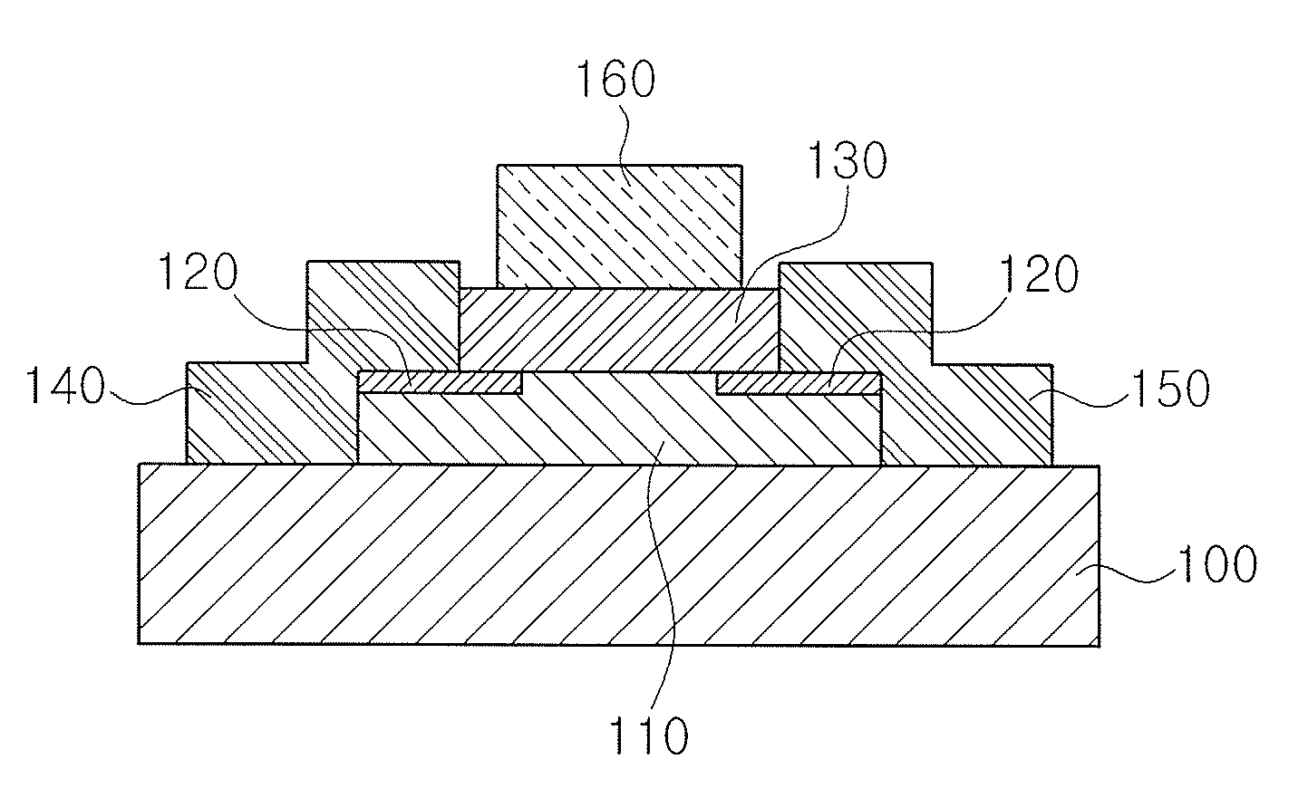
[0058]Hereinafter, the preferred embodiments of the present invention will be described in detail with reference to the accompanying drawings. Herein, the repeated explanation and the detailed description on the well-known function and constitution which may make the gist of the present invention obscure will be omitted. The embodiments of the present invention will be provided in order to clearly describe the present invention to those skilled in the art. Therefore, the shape, size or the like of elements in the drawings may be exaggerated for more definite description. In the drawings, the size and thickness of films (layers) or regions are exaggerated for clarity of the specification.

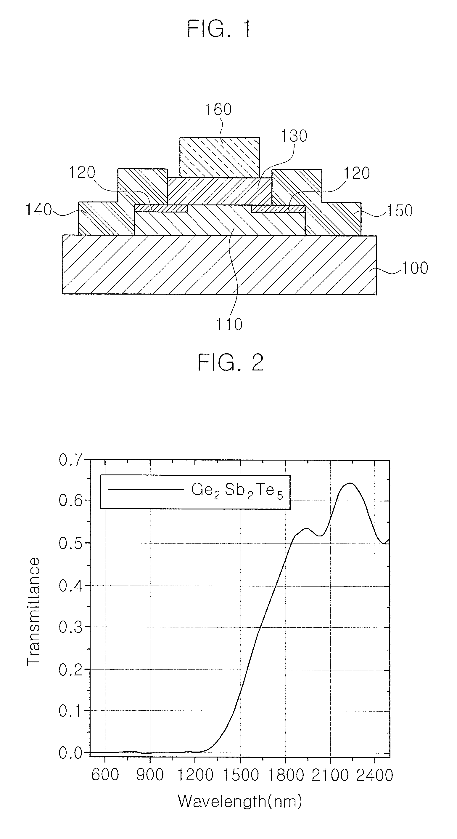
[0059]The present invention uses a chalcogenide layer, which is actively used or can be used as a material for a next generation non-volatile memory device in the field of information storage. As an example of the chalcogenide layer, a GeTe—Sb2Te3 layer (Ge2Sb2Te3, hereinafter, referred to as ‘a GST ...


PUM


Abstract

The present invention provides a doped homojunction chalcogenide thin film transistor and a method of fabricating the same, comprising forming an N-type chalcogenide layer constituting a channel layer on a substrate, forming and patterning a diffusion prevention layer on the upper part of the N-type chalcogenide layer, and forming a P-type chalcogenide layer constituting source and drain regions by depositing and diffusing Te alloy on the N-type chalcogenide layer. With the present invention, a thin film transistor can be fabricated using chalcogenide material having N-type conductivity and chalcogenide material having P-type conductivity.

Description

RELATED APPLICATIONS[0001]The present application claims priority to Korean Patent Application Serial Number 10-2007-0126333, filed on Dec. 6, 2007 and Korean Patent Application Serial Number 10-2008-0114541, filed on Nov. 18, 2008, the entirety of which are hereby incorporated by reference.BACKGROUND OF THE INVENTION[0002]1. Field of the Invention[0003]The present invention relates to a method for manufacturing N-type and P-type chalcogenide materials, a doped homojunction chalcogenide thin film transistor and a method of fabricating the same. More particularly, the present invention relates to a method for manufacturing an N-type chalcogenide material and a P-type chalcogenide material, and a method of fabricating a doped homojunction chalcogenide thin film transistor using the N-type chalcogenide material and P-type chalcogenide material.[0004]This work was supported by the IT R&D program of MIC / IITA [2007-S-032-01, Development for Multiple Platform Supported Mobile Application S...

Claims


Application Information

Patent Timeline
IPC IPC(8): H01L29/786H01L21/06
CPCH01L29/78681H01L29/24
Inventor SONG, KIBONGLEE, SANGSU
Owner ELECTRONICS & TELECOMM RES INST
Why Eureka
Try Eureka