LED Structure

a technology of led structure and led die, which is applied in the direction of semiconductor/solid-state device manufacturing, electrical equipment, semiconductor devices, etc., can solve the problems of increasing the cost of an led, and reducing the cost of a single led

Active Publication Date: 2009-06-11
SEOUL SEMICONDUCTOR
View PDF12 Cites 62 Cited by
  • Summary
  • Abstract
  • Description
  • Claims
  • Application Information

AI Technical Summary

Problems solved by technology

Many high power applications require multiple LEDs to achieve the needed power levels, since individual LEDs are limited to a few watts.
Thus, the cost of many light sources based on LEDs is many times the cost of the individual LEDs.
The cost of an LED is increased by the need to package the LED containing dies prior to installing those dies on printed circuit boards and the like in the final product.
The cost of conventional packaging that relies on wire bonds to connect the dies to an underlying circuit carrier represents a significant fraction of the cost of the final LED.
Unfortunately, the techniques used to increase the conversion efficiency of LEDs are not easily implemented in the flip-chip architecture.
Heat dissipation places a limit on the power level at which an LED operates.
In addition, the LEDs must be mounted on structures that provide heat dissipation, which, in turn, further increases the cost of the light sources.
In addition, the cost of operation of the LED is also inversely proportional to the conversion effic

Method used


Image

  • LED Structure
  • LED Structure
  • LED Structure

Examples


Embodiment Construction

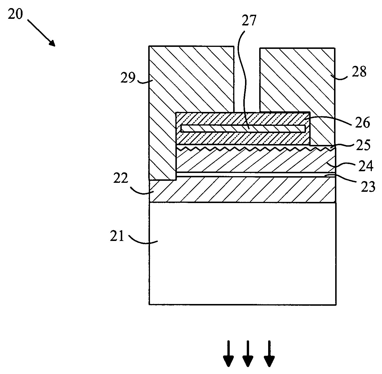
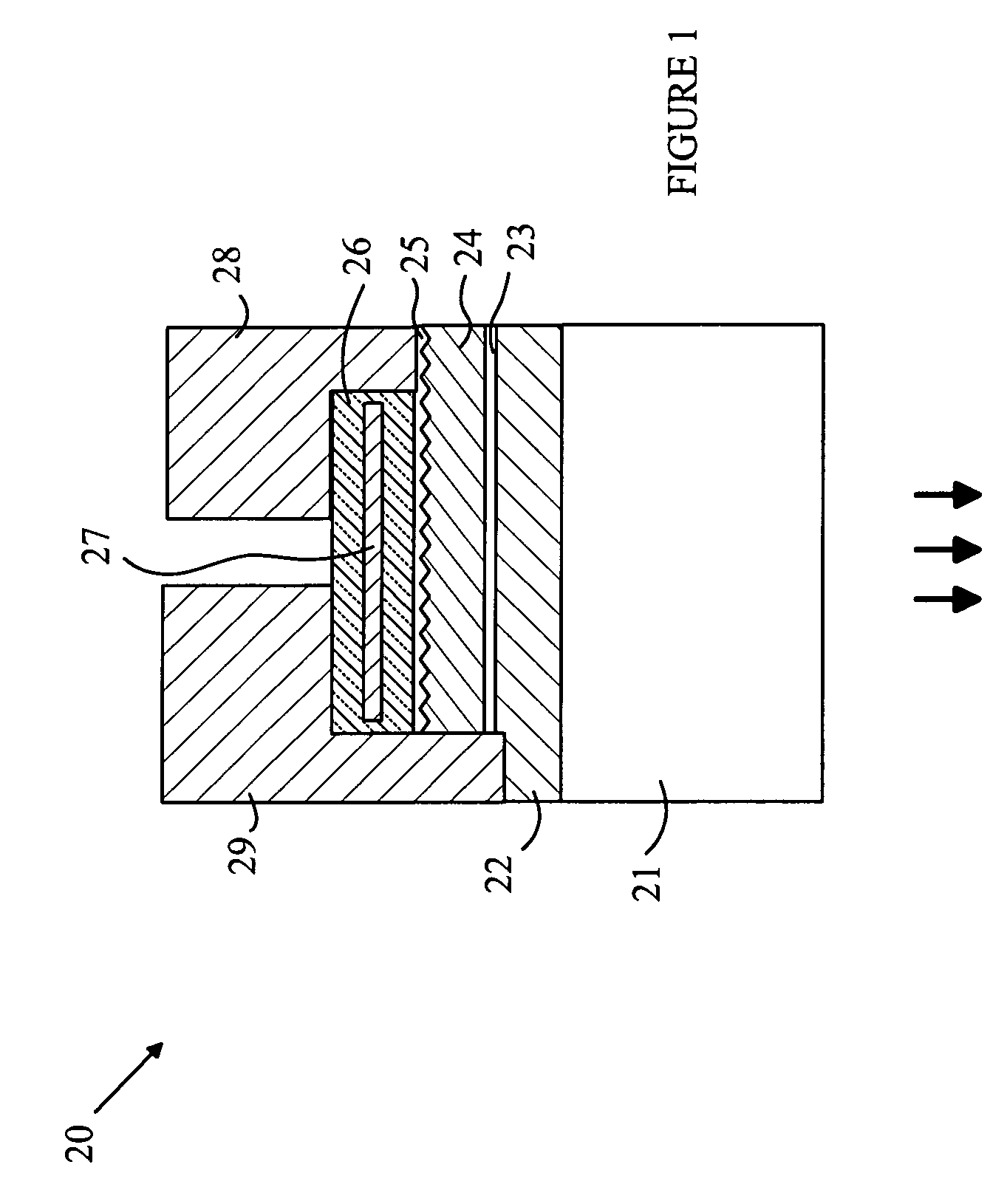
[0020]The manner in which the present invention provides its advantages can be more easily understood with reference to FIG. 1, which is cross-sectional view of an LED according to one embodiment of the present invention. LED 20 is constructed on a sapphire substrate 21 by epitaxially growing a number of layers of GaN family materials. To simplify the following discussion, the layers may be grouped into three layers. An n-type layer 22, an active layer 23, and a p-type layer 24. It is to be understood, however, that each of these layers may include a number of sub-layers that vary in composition with respect to one another. In addition, it should be noted that the layers are not drawn to scale.

[0021]Active layer 23 generates light when holes and electrons from the adjacent layers combine therein. Active layer 23 can be constructed from multiple InGaN layers separated by GaN layers. The precise details of the active region are known to the art, and hence, will not be discussed in det...


PUM


Abstract

A light emitting device, a wafer for making the same, and method for fabricating the same are disclosed. The device and wafer include a first layer of a first conductivity type, an active layer, and a layer of a second conductivity type. The active layer overlies the first layer, the active layer generating light. The second layer overlies the active layer, the second layer having a first surface in contact adjacent to the active layer and a second surface having a surface that includes features that scatter light striking the second surface. A layer of transparent electrically conducing material is adjacent to the second surface and covered by a first layer of a dielectric material that is transparent to the light generated by the active layer. A mirror layer that has a reflectivity greater than 90 percent is deposited on the first layer of dielectric material.

Description

BACKGROUND OF THE INVENTION[0001]Light emitting diodes (LEDs) are an important class of solid-state devices that convert electric energy to light. Improvements in these devices have resulted in their use in light fixtures designed to replace conventional incandescent and fluorescent light sources. The LEDs have significantly longer lifetimes and, in some cases, significantly higher efficiency for converting electric energy to light.[0002]The cost and conversion efficiency of LEDs are important factors in determining the rate at which this new technology will replace conventional light sources and be utilized in high power applications. Many high power applications require multiple LEDs to achieve the needed power levels, since individual LEDs are limited to a few watts. In addition, LEDs generate light in relatively narrow spectral bands. Hence, in applications requiring a light source of a particular color, the light from a number of LEDs with spectral emission in different optical...

Claims


Application Information

Patent Timeline
IPC IPC(8): H01L33/00H01L33/22H01L33/38H01L33/44H01L33/46
CPCH01L33/22H01L33/382H01L33/46H01L33/44H01L33/405H01L33/24
Inventor HASNAIN, GHULAMLESTER, STEVEN D.
Owner SEOUL SEMICONDUCTOR
Why Eureka
Try Eureka