Clock signal generating circuit, display panel module, imaging device, and electronic equipment

a signal generation circuit and clock technology, applied in the direction of automatic control, instruments, electrical equipment, etc., can solve the problems of circuit delay and operating margin, sampling error, and difficulty in panel inclusion

Inactive Publication Date: 2009-06-11
JAPAN DISPLAY WEST
View PDF15 Cites 9 Cited by
  • Summary
  • Abstract
  • Description
  • Claims
  • Application Information

AI Technical Summary

Benefits of technology

[0113]Phase control operations using the clock signal generating circuit 11 will be described with reference to FIG. 10.
[0114]In step S1, at the clock signal generating circuit 11, the phase comparison circuit 29 repeatedly compares the phases of the input clock CLK1 and the output clock CLK2.
[0115]Next, at the clock signal generating circuit 11, determination is made in step S2 regarding whether or not the phase of the output clock CLK2 is advanced as to the phase of the input clock CLK1. More specifically, operations equivalent to this determination processing are executed as operations of supplying the determination output Q2 to the phase relation determining unit 33.
[0116]In the event that a positive result is obtained from the determination processing (i.e., in the event that the phase of the output clock CLK2 is advanced), in step S3 the clock signal generating circuit 11 inverts the phase of the output clock CLK2 by 180° and outputs. Specifically, the phase conversion control signal Pcont with the “H” level is output from the phase relation determining unit 33, and the clock phase is inverted 180° at the phase inversion / non-inversion unit 25.
[0117]On the other hand, in the event that a negative result is obtained from the determination processing in step S2, (i.e., in the event that the phase of the output clock CLK2 is either delayed or synchronized with the input clock CLK1), the current phase relation of the output clock CLK2 is held at the clock signal generating circuit 11. Specifically, the phase conversion control signal Pcont with the “L” level is output from the phase relation determining unit 33, and the clock phase is output at the phase inversion / non-inversion unit 25 as input, with no change.
[0118]Subsequently, in step S4 the clock signal generating circuit 11 adjusts the delay amount of the voltage control type delay line 23 in accordance with the phase difference of the input clock CLK1 and the output clock CLK2. As a result, the phase adjustment capability demanded of the voltage control type delay line 23 is restricted to a range of 180° as to the input clock CLK1.

Problems solved by technology

However, the problem of circuit delay and operating margin still remains for the circuit portion upstream of parallel conversion of the video signals.
Particularly, with recent system displays where the input frequency of video signals is very high, difference in delay between the clock signal generated at the display substrate and the video signal can lead to sampling error.
However, there is a problem with forming or printing active elements making up the clock signal generating circuit on the insulating substrate as thin-film transistors, in that inclusion on the panel is difficult due to the circuit scale thereof.
Particularly, a problem can be easily foreseen where the circuit scale becomes great in the event of configuring portions regarding which delay amount is to be set in the form of digital circuits.
Increased circuit scale leads to poor theoretical yield, which in turn leads to increased costs.

Method used


Image

  • Clock signal generating circuit, display panel module, imaging device, and electronic equipment
  • Clock signal generating circuit, display panel module, imaging device, and electronic equipment
  • Clock signal generating circuit, display panel module, imaging device, and electronic equipment

Examples


first embodiment

A First Embodiment

A-1 Configuration of Display Panel

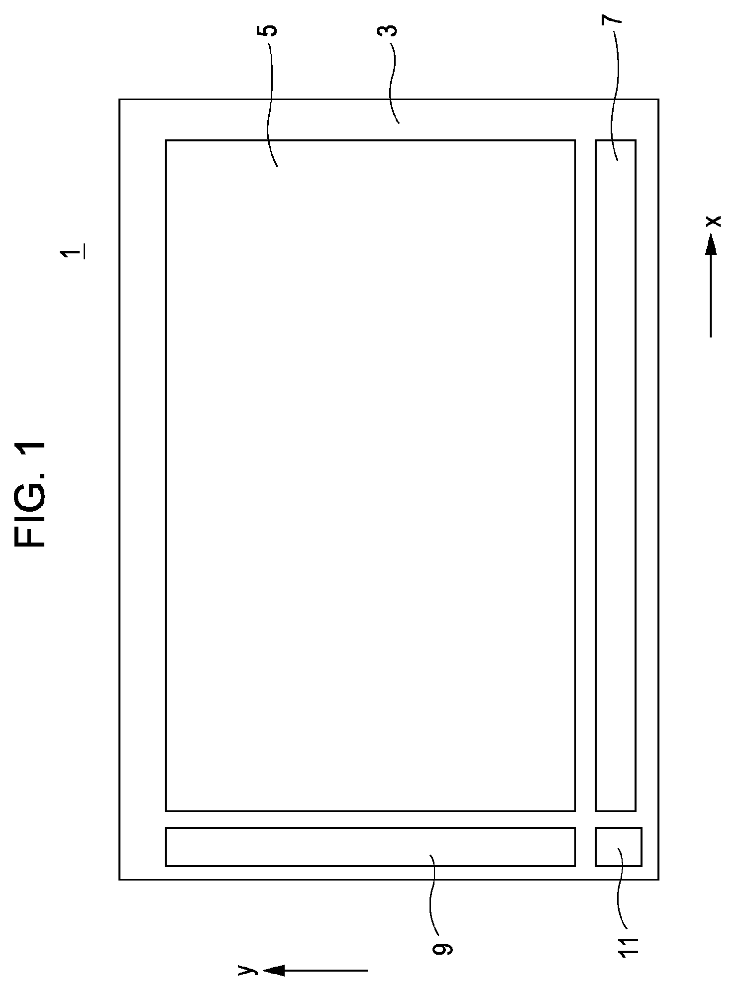
[0078]FIG. 1 illustrates a plan view configuration of a display panel 1 to be described in the present embodiment. In the case of this embodiment, a display region 5 and the peripheral circuits thereof are formed together with the same process on the face of the glass substrate 3. That is to say, we will assume a case wherein the display panel 1 is a system panel.

[0079]Gate lines and signal lines are formed in lattice form on the display region 5 in accordance with the resolution, and pixel circuits are formed at each intersection position thereof. That is to say, the display region 5 has a panel configuration corresponding to the active matrix driving method. Note that gate lines are wiring extending in the x direction of the display region, and signal lines are wiring extending in the y direction of the display region.

[0080]At each pixel circuit, a switching transistor configured of a thin-film transistor, and a retentive capacit...

second embodiment

B Second Embodiment

B-1 Configuration of Display Panel

[0120]FIG. 11 illustrates a plan view configuration of a display panel 51 to be described in the present embodiment. In FIG. 11, components corresponding to FIG. 1 are denoted with the same reference numerals. As shown in FIG. 11, the basic configuration of the display panel 51 is the same as that of the display panel 1 according to the first embodiment, except for the clock signal generating circuit 61.

B-2 Configuration of Clock Signal Generating Circuit (Delay Amount Analog Control Type)

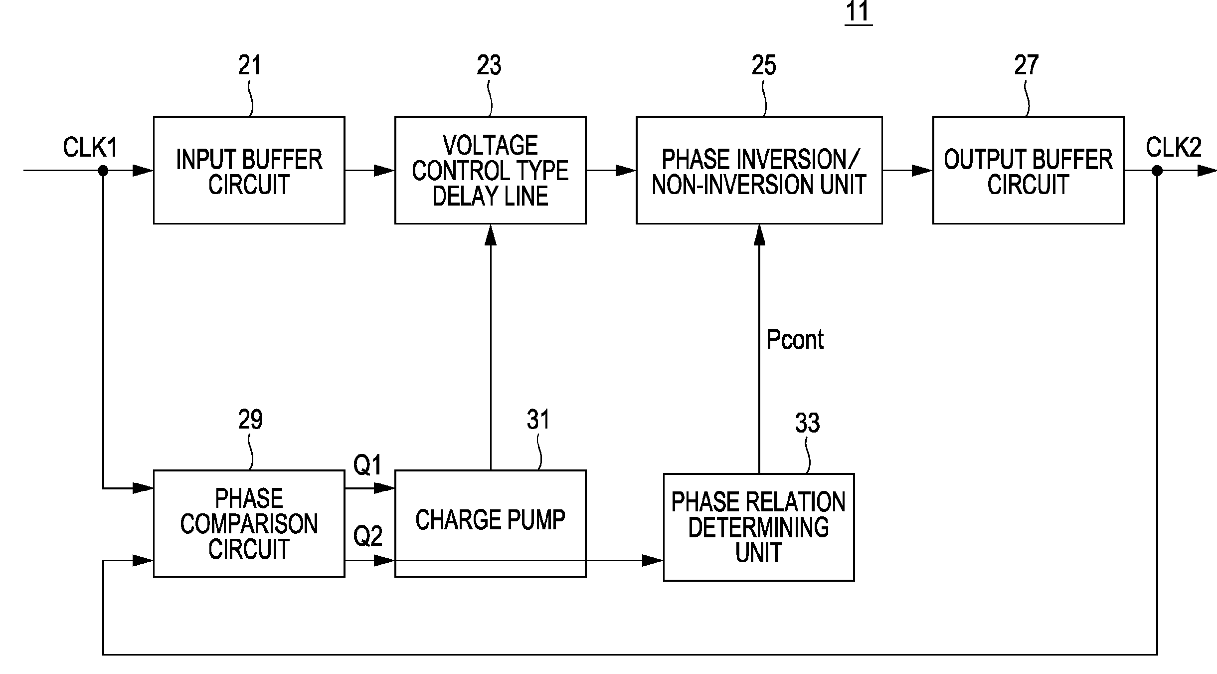
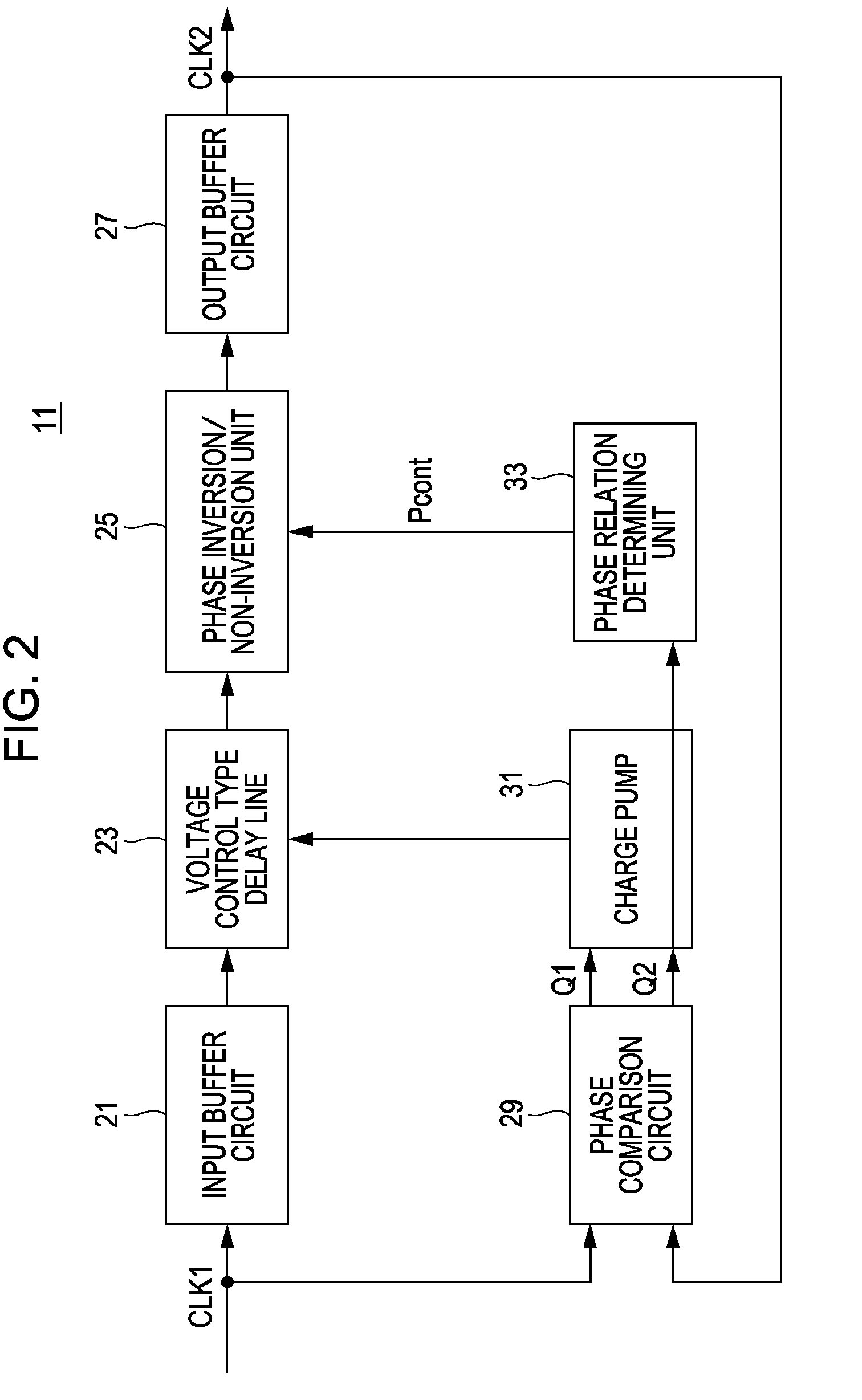
[0121]FIG. 12 illustrates the circuit configuration of the clock signal generating circuit 61 according to the present embodiment. Note that components shown in FIG. 12 which are the same as in FIG. 2 are denoted with the same reference numerals.

[0122]The phase relation determining unit 63 used with this embodiment is a circuit which determines the phase relation between the input clock CLK1 and the output clock CLK2 based on the determination ou...

third embodiment

C Third Embodiment

C-1 Configuration of Display Panel

[0134]FIG. 16 illustrates a plan view configuration of a display panel 71 to be described in the present embodiment. In FIG. 16, components corresponding to FIG. 1 are denoted with the same reference numerals. As shown in FIG. 16, the basic configuration of the display panel 71 is the same as that of the display panel 1 according to the first embodiment, except that the delay line of the clock signal generating circuit 81 is a digital delay line.

C-2 Configuration of Clock Signal Generating Circuit (Delay Amount Digital Control Type)

[0135]FIG. 17 illustrates the circuit configuration of the clock signal generating circuit 81 according to the present embodiment. Note that components which are the same as in FIG. 2 are denoted with the same reference numerals. This clock signal generating circuit 81 is configured of an input buffer circuit 21, a digital delay line 83, a phase inversion / non-inversion unit 25, an output buffer circuit 2...


PUM


Abstract

A delay synchronization loop type clock signal generating circuit includes: a delay line for delaying a first clock signal by a set delay amount and outputting; a delay time length setting unit for setting a delay time length of the delay line, based on phase difference between a second clock signal output from an output terminal and the first clock signal; a phase relation determining unit for determining whether or not the phase relation of the first clock signal and the second clock signal are in a particular phase relation; and a phase inversion/non-inversion unit for performing phase inversion of the first clock signal on a transmission path including the delay line, at the time of detecting the particular phase relation.

Description

CROSS REFERENCES TO RELATED APPLICATIONS[0001]The present invention contains subject matter related to Japanese Patent Application JP 2007-314635 filed in the Japanese Patent Office on Dec. 5, 2007, the entire contents of which are incorporated herein by reference.BACKGROUND OF THE INVENTION[0002]1. Field of the Invention[0003]The present invention relates to a delay synchronization loop type signal generating circuit, and in particular, that which is preferably applicable to cases wherein active elements are formed using thin-film formation techniques and printing techniques. The present invention also can serve as a display panel module, an imaging device, and electronic equipment.[0004]2. Description of the Related Art[0005]As of recent, there is demand for high definition display resolution with not only large-screen displays but also middle-to-small range displays as well. Accordingly, higher frequency input clock signals and video signals are being used. For example, with a sy...

Claims


Application Information

Patent Timeline
Patent Type & Authority Applications(United States)
IPC IPC(8): H03L7/06
CPCG09G3/2096G09G5/008G09G2300/0426G09G2310/0291H03L7/0818H03L7/0812H03L7/0814H03L7/0891G09G2330/021G09G3/20G09G3/30G09G3/36
Inventor SENDA, MICHIRUMIZUHASHI, HIROSHI
Owner JAPAN DISPLAY WEST
Why Eureka
Try Eureka