Variable resistance element, method for producing the same, and nonvolatile semiconductor storage device

Inactive Publication Date: 2009-06-11
SHARP KK +1
View PDF17 Cites 54 Cited by
  • Summary
  • Abstract
  • Description
  • Claims
  • Application Information

AI Technical Summary

Benefits of technology

[0015]The present invention has been accomplished in view of the problem above, and an object of the present invention is to provide a variable resistant element in which a forming voltage for providing a conductive section

Problems solved by technology

However, it is difficult for these elements to be superior to the flash memory in terms of low bit-cost and small cell area.
However, the perovskite material has a problem in compatibility with a general semiconductor proce

Method used


Image

  • Variable resistance element, method for producing the same, and nonvolatile semiconductor storage device
  • Variable resistance element, method for producing the same, and nonvolatile semiconductor storage device
  • Variable resistance element, method for producing the same, and nonvolatile semiconductor storage device

Examples


referential example

[0046]FIG. 15 is a cross-sectional view showing a structure of a conventional variable resistance element 3 before a forming process. Note that the forming is specifically described later. As shown in FIG. 15, the variable resistance element 3 has electrodes 11 and 12 and a metal oxide layer 10 made of a metal oxide material sandwiched between the electrodes 11 and 12.

[0047]Briefly described below is an effect that the variable resistance element 3 achieves. The variable resistance element 3 achieves such an effect that an electrical resistance between the electrodes 11 and 12 changes in response to a threshold voltage applied to the electrodes 11 and 12. Specifically, the electrical resistance between the electrodes 11 and 12 becomes either one of low resistance state and high resistance state in response to the applied threshold voltage.

[0048]In the descriptions hereinafter, a low resistance operation by which the electrical resistance between the electrodes 11 and 12 of the varia...

first embodiment

[0055]A variable resistance element 1 in accordance with the present invention is for solving the above-mentioned problem of the variable resistance element 3 according to the conventional technique. Specifically, the variable resistance element 1 is for reducing a forming voltage at the time of forming without causing a leakage current to increase.

[0056]A variable resistance element 1 in accordance with First Embodiment of the present invention is described below with reference to FIGS. 1 through 9.

[0057](Arrangement of Variable Resistance Element 1)

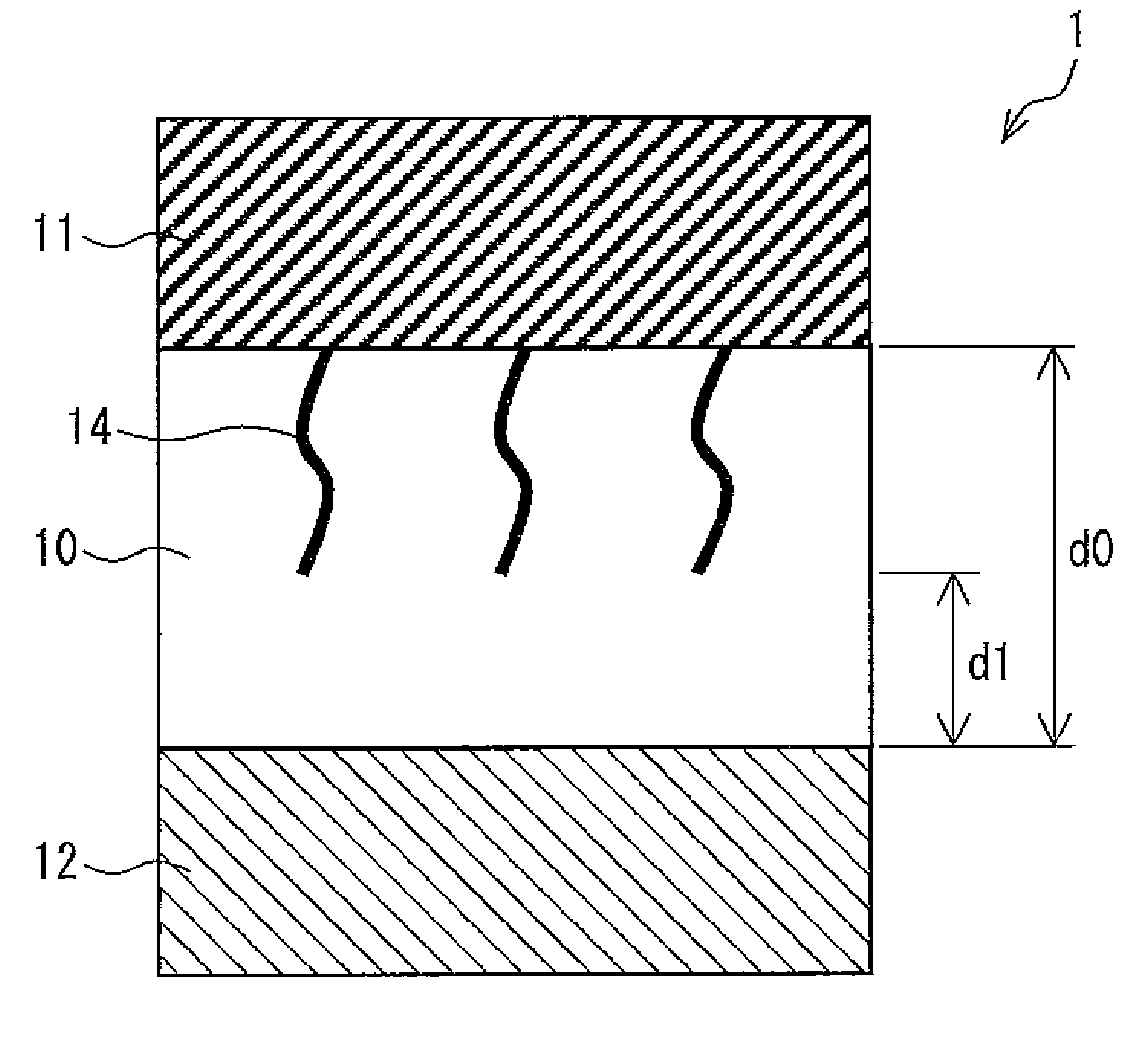
[0058]FIG. 1 is a cross-sectional view showing a structure of a variable resistance element 1 in accordance with First Embodiment. As shown in FIG. 1, the variable resistance element 1 has electrodes 11 and 12, and a metal oxide layer 10 made of a metal oxide material sandwiched between the electrodes 11 and 12. Further, the variable resistance clement 1 has, inside the metal oxide layer 10, a low resistance material 14 having a lower e...

second embodiment

[0096]A nonvolatile semiconductor storage device 4 (hereinafter referred to as “storage device”) in accordance with Second Embodiment of the present invention is described below with reference to FIGS. 13 and 14.

[0097]First, an arrangement of the storage device 4 is described with reference to FIG. 13. FIG. 13 is a block diagram showing the arrangement of the storage device 4.

[0098]As shown in FIG. 13, the storage device 4 has a memory cell array 40, a bit line decoder 41, a word line decoder 42, a voltage switching circuit 44, a readout circuit 45, a voltage generating circuit 46, and a control circuit 43.

[0099]An arrangement inside the memory cell array 40 is described below with reference to FIG. 14. FIG. 14 is a schematic view showing the arrangement of the memory cell array 40.

[0100]As shown in FIG. 14, the memory cell array 40 has a plurality of variable resistance elements 1 or 2, described in First Embodiment, as memory cells 50. The plurality of the memory cells 50 are arra...


PUM

PropertyMeasurementUnit
Electrical resistanceaaaaaaaaaa
Grain boundaryaaaaaaaaaa

Abstract

The variable resistance element of the present invention is a variable resistance element having an electrode, the other electrode, and a metal oxide material sandwiched between the electrodes and having an electrical resistance, between the electrodes, changing reversibly in response to a voltage applied between the electrodes. The variable resistance element further includes, inside the metal oxide material, a low resistance material having a lower electrical resistance than the metal oxide material and being out of contact with at least either one of the electrodes. This makes it possible to reduce a forming voltage for providing a conductive section inside the metal oxide material, without causing a leakage current to increase.

Description

[0001]This Nonprovisional application claims priority under U.S.C. §119(a) on Patent Application No. 317733 / 2007 filed in Japan on Dec. 7, 2007, the entire contents of which are hereby incorporated by reference.FIELD OF THE INVENTION[0002]The present invention relates to a variable resistance element having an electrical resistance which reversibly changes in response to a change in voltage applied to a metal oxide material sandwiched between two electrodes, a method for producing the variable resistance element, and a nonvolatile semiconductor storage device having the variable resistance element served as a memory cell.BACKGROUND OF THE INVENTION[0003]Recently, a nonvolatile semiconductor storage device represented by a flash memory has been remarkably developed in capacity. These days, a product having approximately 4 gigabyte capacity is marketed for about several tens of thousands yen. In particular, a mobile or transportable memory such as a USB memory is increasing in commerc...

Claims


Application Information

Patent Timeline
IPC IPC(8): G11C11/21H01C7/10H01C17/00
CPCG11C8/08G11C13/0007G11C13/0028G11C2013/0083G11C2213/32G11C2213/56Y10T29/49082H01C7/108H01L45/04H01L45/1233H01L45/1246H01L45/146H01L45/1658G11C2213/77H10N70/20H10N70/828H10N70/046H10N70/8833H10N70/826
Inventor TAMAI, YUKIOHOSOI, YASUNARIAWAYA, NOBUYOSHIOHNISHI, SHIGEOISHIHARA, KAZUYASHIMA, HISASHITAKANO, FUMIYOSHIAKINAGA, HIROYUKI
Owner SHARP KK
Why Eureka
Try Eureka