Method of manufacturing a semiconductor device

a manufacturing method and semiconductor technology, applied in the direction of semiconductor/solid-state device details, coatings, chemical vapor deposition coatings, etc., can solve the problems of increasing the contact resistance between the barrier metal film and the natural oxide film deposited on the surface of the nickel silicide layer, and the inability to completely remove the natural oxide film

Inactive Publication Date: 2009-06-11
RENESAS ELECTRONICS CORP
View PDF7 Cites 21 Cited by
  • Summary
  • Abstract
  • Description
  • Claims
  • Application Information

AI Technical Summary

Benefits of technology

[0016]The following is a brief description of an effect achievable by

Problems solved by technology

However, even when the titanium film functioning as the reductant is formed over the nickel silicide layer, a natural oxide film deposited on the surface of the nickel silicide layer can

Method used


Image

  • Method of manufacturing a semiconductor device
  • Method of manufacturing a semiconductor device
  • Method of manufacturing a semiconductor device

Examples


Embodiment Construction

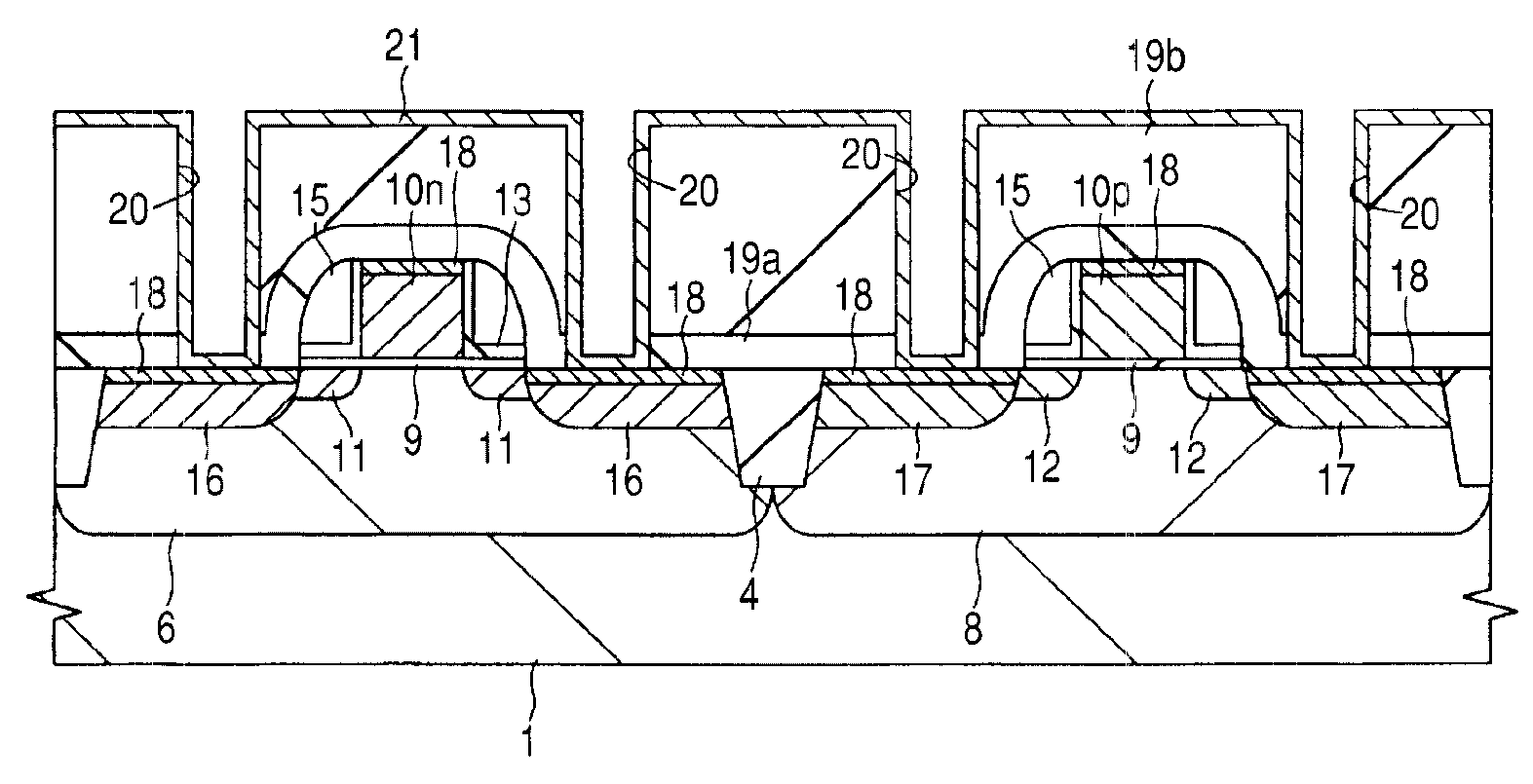
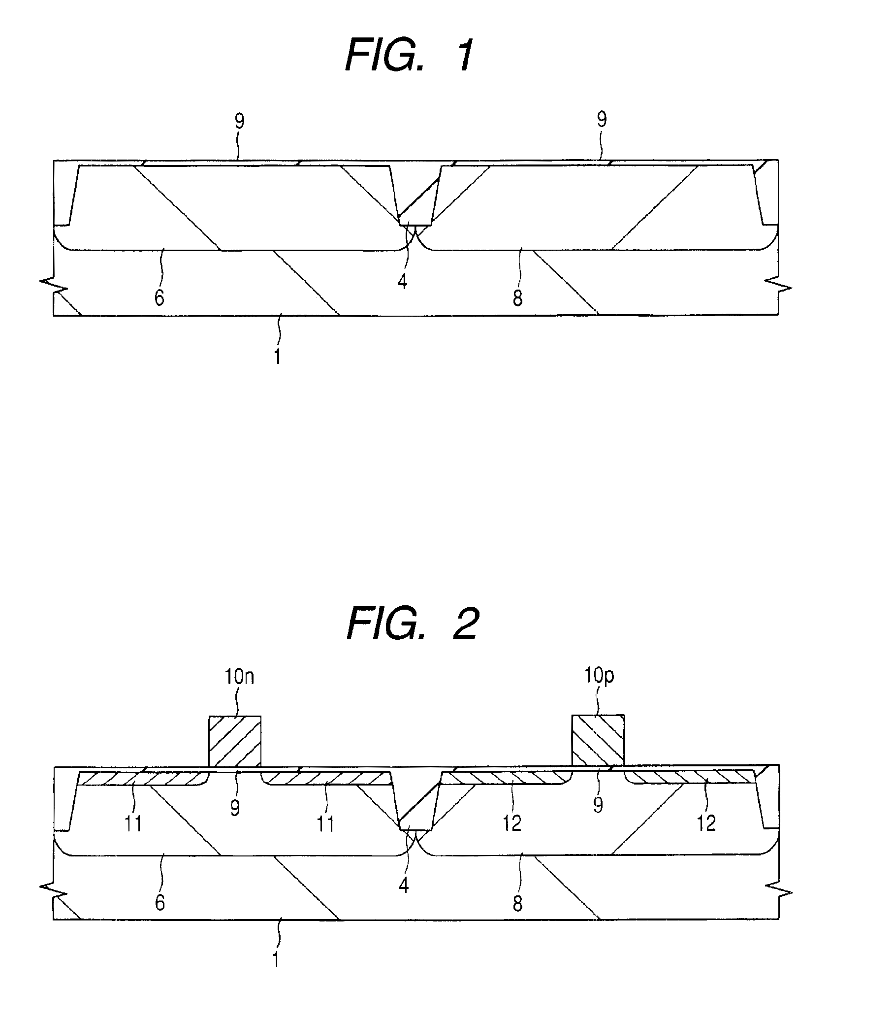
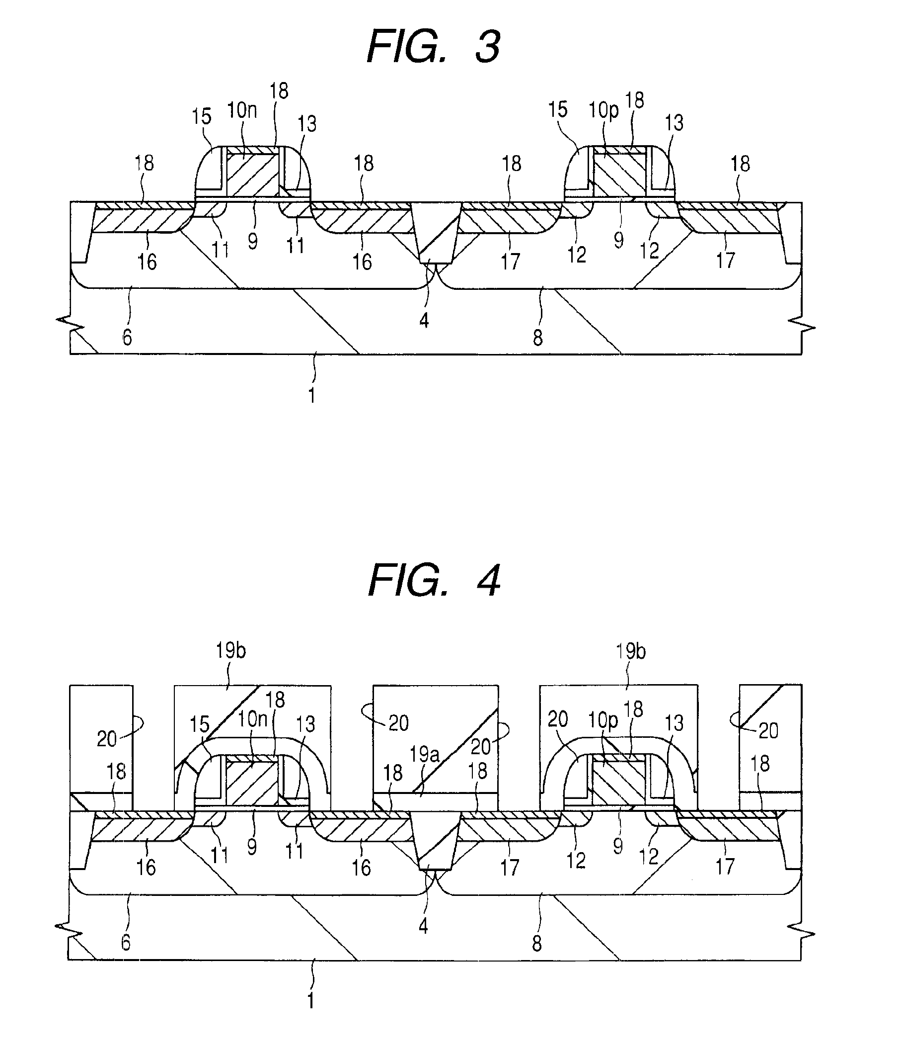
[0043]If necessary for the sake of convenience, the present embodiment will be described by dividing it into a plurality of sections or implementations. However, they are by no means irrelevant to each other unless shown particularly explicitly, and are mutually related to each other such that one of the sections or implementations is a variation or a detailed or complementary description of some or all of the others. When the number and the like of elements (including the number, numerical value, amount, and range thereof) are referred to in the present embodiment, they are not limited to specific numbers unless shown particularly explicitly or unless they are obviously limited to specific numbers in principle. The number and the like of the elements may be not less than or not more than specific numbers. It will easily be appreciated that, in the present embodiment, the components thereof (including also elements, steps, and the like) are not necessarily essential unless shown par...


PUM

PropertyMeasurementUnit
Temperatureaaaaaaaaaa

Abstract

A technology is provided which allows, in a coupling portion obtained by burying a conductive material within a coupling hole bored in an insulating film, the removal of a natural oxide film on the surface of a silicide layer which is present at the bottom portion of the coupling hole. A coupling hole is bored in an interlayer insulating film (first and second insulating films) to expose the surface of a nickel silicide layer at the bottom portion of the coupling hole. Then, reduction gases including a HF gas and a NH3 gas is supplied to the principal surface of a semiconductor wafer to form a product by a reduction reaction, and remove the natural oxide film on the surface of the nickel silicide layer. At this time, the flow rate ratio (HF/NH3 gas flow rate ratio) between the NF gas and the NH3 gas is adjusted to be more than 1 and not more than 5. Preferably, the temperature of the semiconductor wafer is adjusted to be not more than 30° C. Thereafter, a heating process is performed at 400° C. to the semiconductor wafer to remove the product remaining on the principal surface of the semiconductor wafer, and subsequently form a barrier metal film.

Description

CROSS-REFERENCE TO RELATED APPLICATIONS[0001]The disclosure of Japanese Patent Application No. 2007-315522 filed on Dec. 6, 2007 including the specification, drawings and abstract is incorporated herein by reference in its entirety.BACKGROUND OF THE INVENTION[0002]The present invention relates to a technology for manufacturing a semiconductor device and, more particularly, to a technology which is effective when applied to a manufacturing process of a semiconductor device in which a metal film is buried within a coupling hole bored in an insulating film via a barrier metal film.[0003]In Japanese Unexamined Patent Publication No. 2004-363402, a method is disclosed which forms a Ti layer at least on the inner wall and bottom portion of a contact hole extending through an insulating layer, further forms a TiN layer over the Ti layer by nitriding the Ni layer using N radicals, and then buries a conductive layer within the contact hole (see Patent Document 1).[0004]In Japanese Unexamined...

Claims


Application Information

Patent Timeline
IPC IPC(8): H01L21/44H01L21/31
CPCC23C16/14C23C16/34H01L2924/0002C23C16/4401H01L21/02063H01L21/28518H01L21/28556H01L21/76814H01L21/76843H01L21/76846H01L21/76856H01L21/76862H01L21/76876H01L21/76877H01L23/485H01L23/53266H01L2924/00
Inventor HAYASHI, TAKESHIFUTASE, TAKUYA
Owner RENESAS ELECTRONICS CORP
Why Eureka
Try Eureka