Semiconductor devices and method of testing same

a technology of semiconductor devices and semiconductors, applied in the direction of individual semiconductor device testing, semiconductor/solid-state device testing/measurement, instruments, etc., can solve the problems of electric failure detection at a speed which is increasingly lower, the detection resolution cannot but be increasingly smaller, and the size of the semiconductor devi

Inactive Publication Date: 2009-06-18
EBARA CORP
View PDF3 Cites 91 Cited by
  • Summary
  • Abstract
  • Description
  • Claims
  • Application Information

AI Technical Summary

Problems solved by technology

However, the pitch of wires in semiconductor devices is increasingly smaller year by year, so that the detection resolution cannot but be increasingly smaller in association therewith.
As a result, a problem arises that electric failures are detected at speeds which are increasingly lower year by year.
However, the method which irradiates contacts with an electron beam EB to sequentially test the contacts one by one in this manner performs the scan using the fine electron beam EB, thus giving rise to a problem that an extremely long time is required to scan the overall surface of semiconductor.
However, though the conventional testing method described in connection with FIGS. 3(A), 3(B), 3(C) can produce predetermined effects in improving the detection sensitivity and increasing the testing speed, this method cannot sufficiently support the trend of increasingly larger areas of wafers, advanced in the Si LSI manufacturing, and miniaturization every two to three years.

Method used


Image

  • Semiconductor devices and method of testing same
  • Semiconductor devices and method of testing same
  • Semiconductor devices and method of testing same

Examples


first embodiment

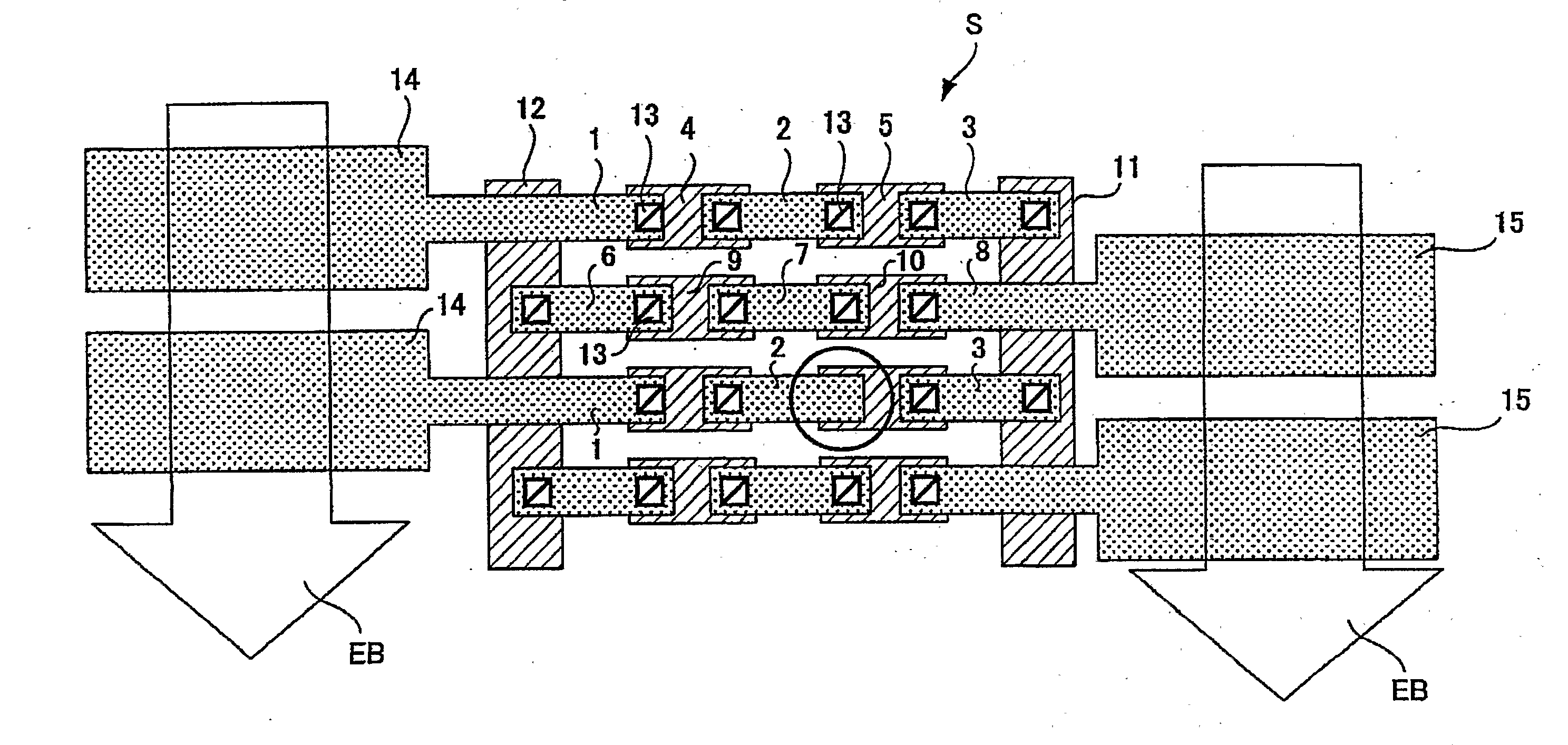
[0188]FIG. 4 illustrates a semiconductor device according to the present invention. In FIG. 4, a semiconductor device S has a semiconductor structure which comprises multiple basic structures, each including a via chain for connecting an upper layer wire and a lower layer wire through a via, which are two-dimensionally arranged on a periodic basis. Specifically, the basic structure of the semiconductor device S includes the following components, and FIG. 4 illustrates two basic structures:

[0189](1) a first row wire which has a plurality of wires 1, 2, 3 arranged at predetermined intervals in a row direction (in a left-to-right direction in FIG. 1) in a first layer;

[0190](2) wires 4, 5 formed in a lower layer at positions at which they can connect adjacent ends of the wires 1, 2, 3 in the first layer;

[0191](3) a second row wire which has a plurality of wires 6, 7, 8 arranged at predetermined intervals in the row direction, disposed in the first layer in parallel with the first row wi...

second embodiment

[0207]Since the second embodiment has the structure as described above, a broken point b, if occurring on the row wire 21 which should be essentially at the ground potential, will cause the right side from the broken point b, i.e., wires connected to the conductor 23 to transition to an open potential (floating potential). Therefore, when the conductors 26 are scanned using an electron beam EB, the conductors at the ground potential differ in the secondary electron emission amount from the conductors at the open potential. By taking advantage of this phenomenon, it is possible to detect the presence or absence of a line break on a row wire which should be essentially at the ground potential. Likewise, in this embodiment, since the conductors are formed on every other row wires at first and second ends, respectively, these conductors are arranged at a wiring pitch reduced to one-half of the row wires. Accordingly, since the width in the column direction is two times wider, they can b...

third embodiment

[0211]FIGS. 7(A) and 7(B) are diagrams generally illustrating a semiconductor device according to the present invention for effectively detecting a location at which a short has occurred, as described above. FIG. 7(A) is a diagram illustrating a mutual positional relationship among components which make up a basic structure of a semiconductor device S, and FIG. 7(B) illustrates a cross-sectional view taken along a line B-B in FIG. 7(A). The semiconductor device S according to this embodiment employs the illustrated structure as a basic structure, and has a semiconductor structure which comprises a large number of the basic structures which are two-dimensionally arranged on a periodic basis.

[0212]As illustrated, the basic structure of the semiconductor device comprises the following components:

[0213](1) a first pair of gate electrodes 42, 43 elongated in the row direction, and formed on a thick SiO2 substrate (STI (Shallow Trench Isolation)) 41 through a gate insulating film 32;

[0214...


PUM


Abstract

There are provided a semiconductor device having a pattern which allows electric failures to be sensitively detected at high speeds, and a method of testing the same. In one embodiment, the semiconductor device comprises a pair of row wires including a plurality of first wires arranged in a first layer at predetermined intervals in a row direction, where the first wires have ends connected to second wires arranged in a second layer at a predetermined intervals through vias, and the first wire and second wire are at the same potential. In the pair of row wires, a first wire positioned at a right end of one row wire is connected to a first conductor, and a first wire positioned at a left end in the other row wire is connected to a second conductor. By sequentially scanning the first conductor and second conductor using an electron beam, a change in the amount of emitted secondary electrons due to a difference in potential between these conductors is detected to detect electric anomalies.

Description

TECHNICAL FIELD[0001]The present invention relates to semiconductor devices and methods of testing the same. Particularly, the present invention relates to a variety of Si LSI's such as a dynamic random access memory (DRAM), a flash memory, logic LSI's and the like, as well as structures for the semiconductors and methods of testing the same, which are capable of highly sensitively detecting, in a short time, defects such as a wire short failure, a wire open failure, a self aligned contact short failure and the like which occur due to defective dimensions of wire widths and contact diameters in those Si LSI's.BACKGROUND ART[0002]A variety of proposals have been conventionally made for detecting electric failures which are found in wires of semiconductor devices. An example of them is a voltage contrast method described in Laid-open Japanese Patent applications Nos. 11-27066 and 2000-223540, which will be now described with reference to FIG. 1. In FIG. 1, a semiconductor device has a...

Claims


Application Information

Patent Timeline
Patent Type & Authority Applications(United States)
IPC IPC(8): H01L23/522G01R31/302
CPCG01R31/2884G11C29/025G11C29/02G01R31/307G01R31/302H01L21/768H01L22/00
Inventor KAGA, TORUNAITO, YOSHIHIKOTSUNEOKA, MASATOSHITERAO, KENJINOJI, NOBUHARUTAJIMA, RYO
Owner EBARA CORP
Why Eureka
Try Eureka