High-k dielectric and metal gate stack with minimal overlap with isolation region and related methods

Inactive Publication Date: 2009-06-18
IBM CORP
View PDF6 Cites 62 Cited by
  • Summary
  • Abstract
  • Description
  • Claims
  • Application Information

AI Technical Summary

Benefits of technology

[0006]A high-k dielectric and metal gate stack with minimal overlap with an adjacent oxide isolation region and related methods are disclosed. One embodiment of the gate stack includes a high dielectric constant (high-k) dielectric layer, a tuning layer and a metal layer positioned over an active region defined by an oxide isolation region in a substrate, wh

Problems solved by technology

One challenge for this technology is that narrow width short channel transistors utilizing high-k dielectrics and metal gate electrodes in traditional CMOS gate-first processing suffer from unintentional re-growth of silicon oxide in the active regions.
Consequently, the oxygen interacts with the silicon in the active region to form (re-grow) silicon oxide like dielectrics, which disadvantageously increases the equivalent oxide thickness (EOT) of the gate dielectric, i.e., the thickness of the gate dielectric is that of the high-k dielectric plus the re-grown silicon oxide i

Method used


Image

  • High-k dielectric and metal gate stack with minimal overlap with isolation region and related methods
  • High-k dielectric and metal gate stack with minimal overlap with isolation region and related methods
  • High-k dielectric and metal gate stack with minimal overlap with isolation region and related methods

Examples


Embodiment Construction

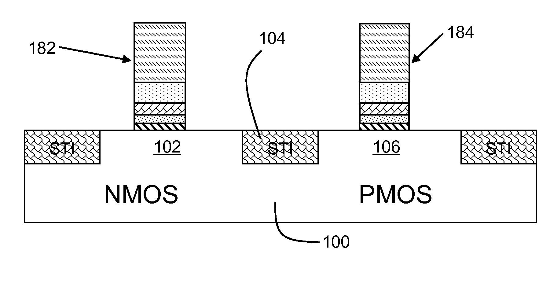
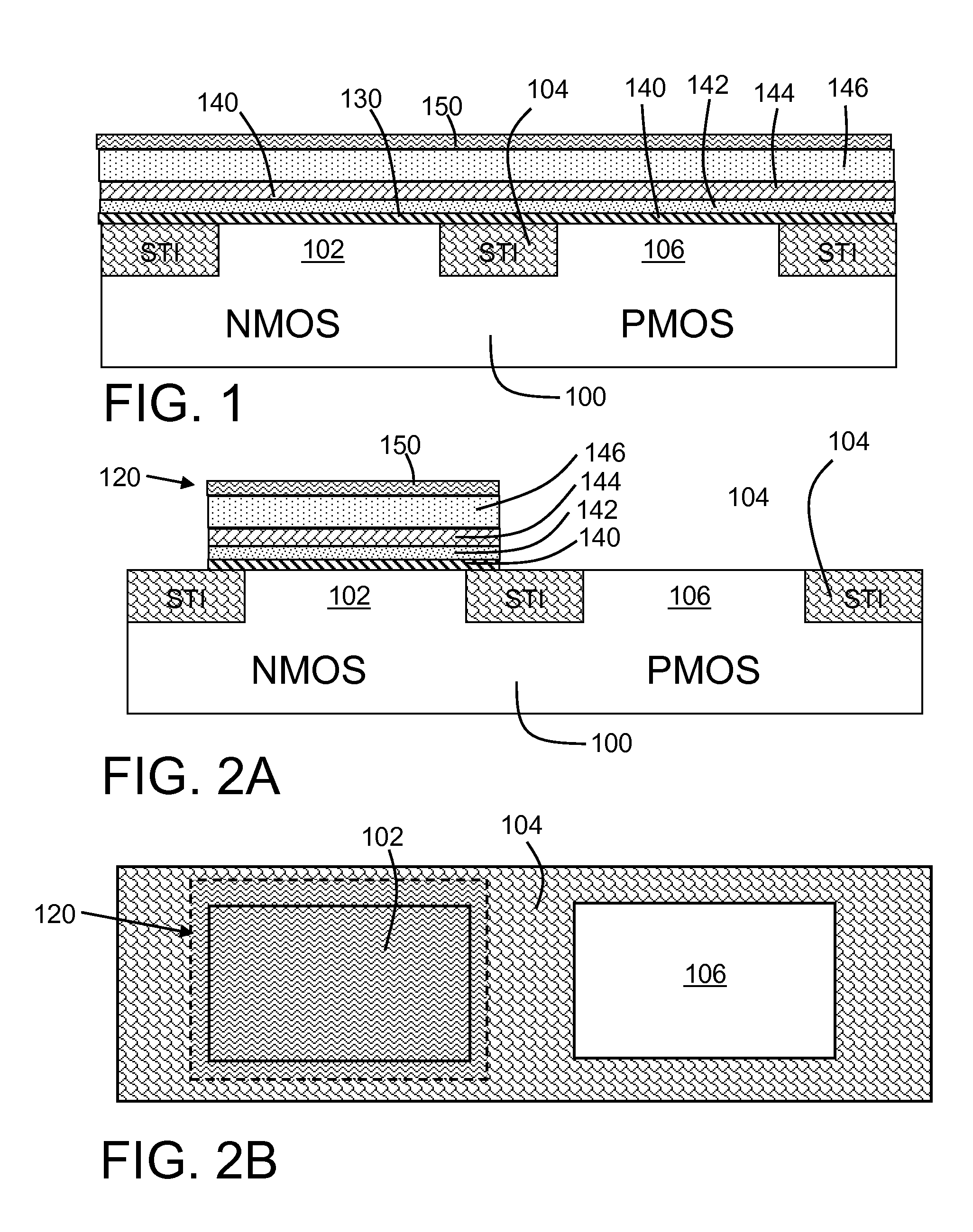
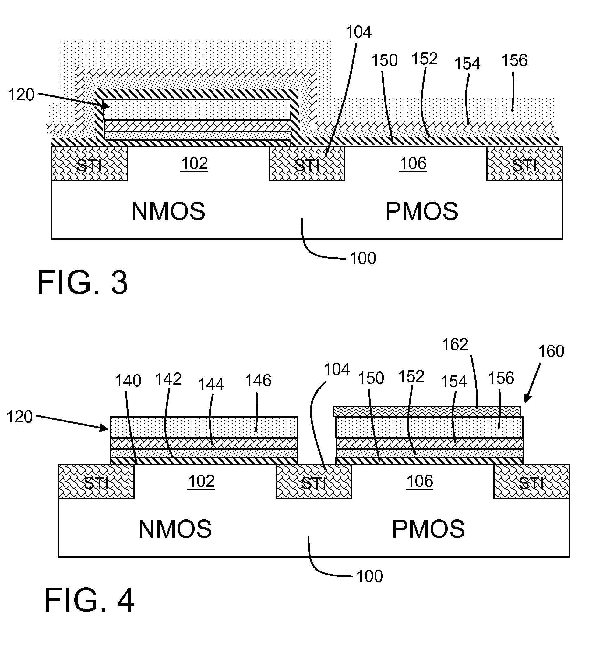
[0014]Conventional approaches to forming high dielectric constant (high-k) dielectric and metal gate stacks attribute the above-described silicon oxide re-growth in active regions to oxide from the high-k gate dielectrics (which typically include an oxide such as hafnium oxide (HfO2)) that are positioned over the active region. However, this disclosure identifies a root cause of the silicon oxide re-growth as the overlap between the gate stack and the adjacent oxide isolation regions. In particular, while the high-k dielectrics indeed play a direct part in the silicon oxide re-growth, a more significant effect is created in how the high-k dielectrics tend to scavenge oxygen (O2) from the adjacent isolation regions, and pipe it into the active silicon regions adjacent to the isolation regions. It is this overlap area that determines the amount of silicon oxide regrowth. According to this disclosure, the overlap is restricted to minimize the silicon oxide re-growth.

[0015]Referring to ...


PUM


Abstract

A high-k dielectric and metal gate stack with minimal overlap with an adjacent oxide isolation region and related methods are disclosed. One embodiment of the gate stack includes a high dielectric constant (high-k) dielectric layer, a tuning layer and a metal layer positioned over an active region defined by an oxide isolation region in a substrate, wherein an outer edge of the high-k dielectric layer, the tuning layer and the metal layer overlaps the oxide isolation region by less than approximately 200 nanometers. The gate stack and related methods eliminate the regrowth effect in short channel devices by restricting the amount of overlap area between the gate stack and adjacent oxide isolation regions.

Description

BACKGROUND[0001]1. Technical Field[0002]The disclosure relates generally to integrated circuit (IC) fabrication, and more particularly, to a high dielectric constant (high-k) dielectric and metal gate stack and related methods.[0003]2. Background Art[0004]In the integrated circuit (IC) fabrication industry, metal gate electrodes are being pursued for, for example, the 45 nanometer (nm) and 32 nm technology nodes as a replacement for doped polysilicon (poly-Si) gate electrodes for a number of reasons. A metal gate electrode includes a high dielectric constant (high-k) dielectric within a metal gate stack. One reason, among many, that this technology is being pursued is to enable gate length scaling. Thinner gate dielectrics enable the gate length to be scaled which in turn improves the performance and density of integrated circuits. The best known self aligned process flows for complementary metal oxide semiconductor (CMOS) fabrication with the high-k dielectrics and metal gate stack...

Claims


Application Information

Patent Timeline
IPC IPC(8): H01L29/49H01L21/283
CPCH01L21/28123H01L21/823842H01L29/518H01L29/513H01L29/517H01L21/823857
Inventor CHUDZIK, MICHAEL P.HENSON, WILLIAM K.MO, RENEE T.SLEIGHT, JEFFREY W
Owner IBM CORP
Why Eureka
Try Eureka