Leadframe having die attach pad with delamination and crack-arresting features

Active Publication Date: 2009-06-18
NAT SEMICON CORP
View PDF38 Cites 73 Cited by
  • Summary
  • Abstract
  • Description
  • Claims
  • Application Information

AI Technical Summary

Benefits of technology

[0010]In some preferred embodiments, the pedestals do not underlie any edge regions of the die. The size and geometry of the pedestals may vary widely. By way of example, circular, oval, substantially rectangular, square, diamond shaped, and other pedestal geometries may be used. In some embodiments, the corners of the die attach pad may be rounded to further reduce stress concentrations.
[0011]The die attach pad may also optionally include one or more bus bars defined in the top surface of the die attach pad. In some embodiments, the die is electrically connected to at least one bus bar such that the die attach pad functions as a contact. When multiple bus bars are employed, recessed regions may be provided between adjacent bus bars to facilitate the flow of encapsulant around the bus bars and into recessed regions of the die attach pad that are not filled by adhesive material.

Problems solved by technology

During testing and operation, packages may be repeatedly exposed to temperature cycling and other environmental stresses.
By way of example, some testing protocols require cycling between temperatures as high as 125° C. and as low as −40° C. Such extreme changes in temperature may lead to delamination of the die from the die attach pad, which in turn may cause poor thermal performance, die cracking, the shearing of wirebonds attached to the die pad and other problems.
As noted earlier, the testing and operation of a package can damage the integrity of the package.
Such stresses may result in delamination or cracking.
The shifting of die attach pad 105 relative to molding material 117 of FIG. 1C may cause a number of problems.
Additionally, delamination between layers of the package may create air gaps within the package.
Air gaps tend to reduce the thermal performance of package 119.

Method used


Image

  • Leadframe having die attach pad with delamination and crack-arresting features
  • Leadframe having die attach pad with delamination and crack-arresting features
  • Leadframe having die attach pad with delamination and crack-arresting features

Examples


Embodiment Construction

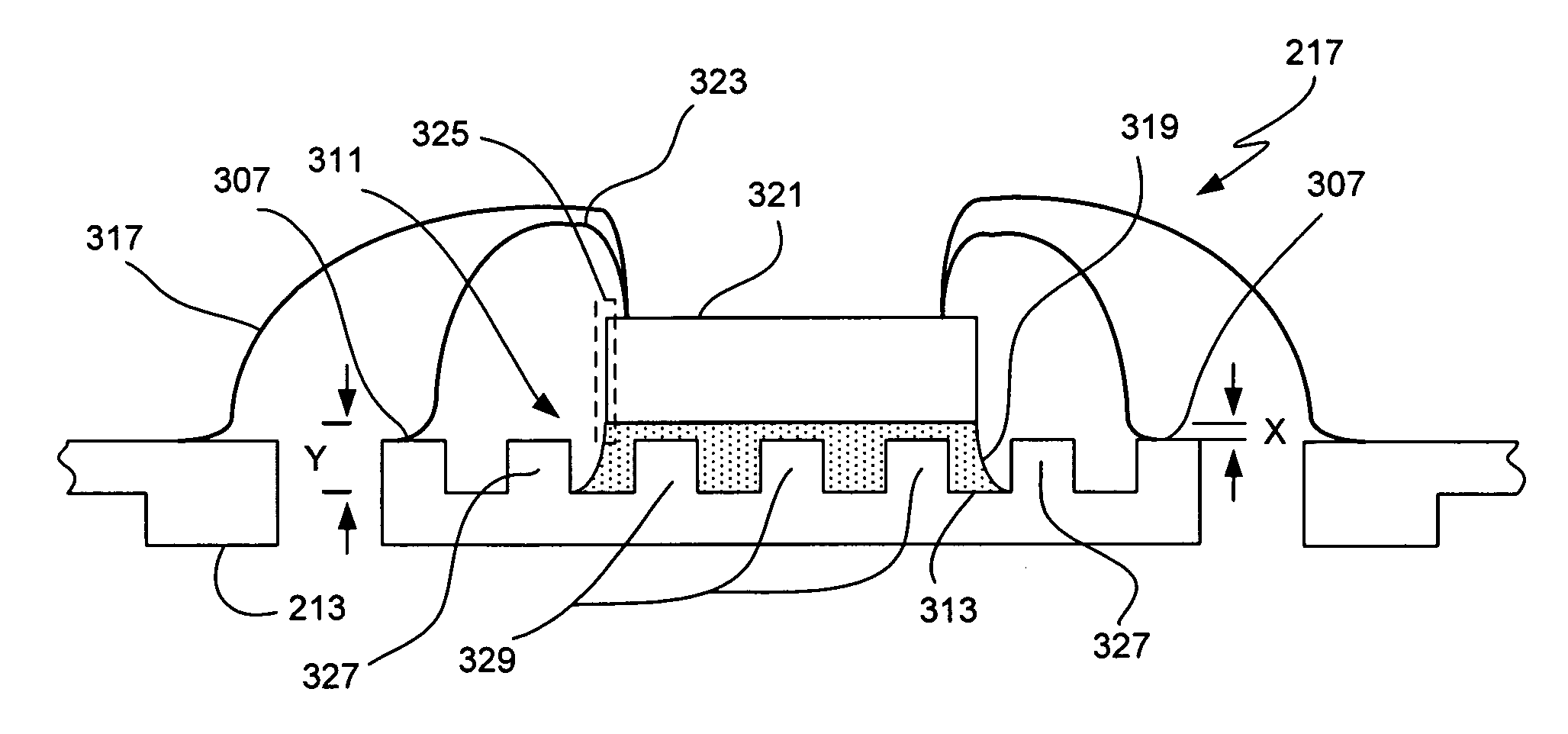
[0032]The present invention relates generally to the packaging of integrated circuits. As explained in the background section, the testing and operation of an integrated circuit (IC) package may subject the package to temperature extremes and other stresses. Such stresses may cause delamination and degrade the performance of the package. The present invention provides a semiconductor package and a method designed to help counteract such stresses and reduce delamination.

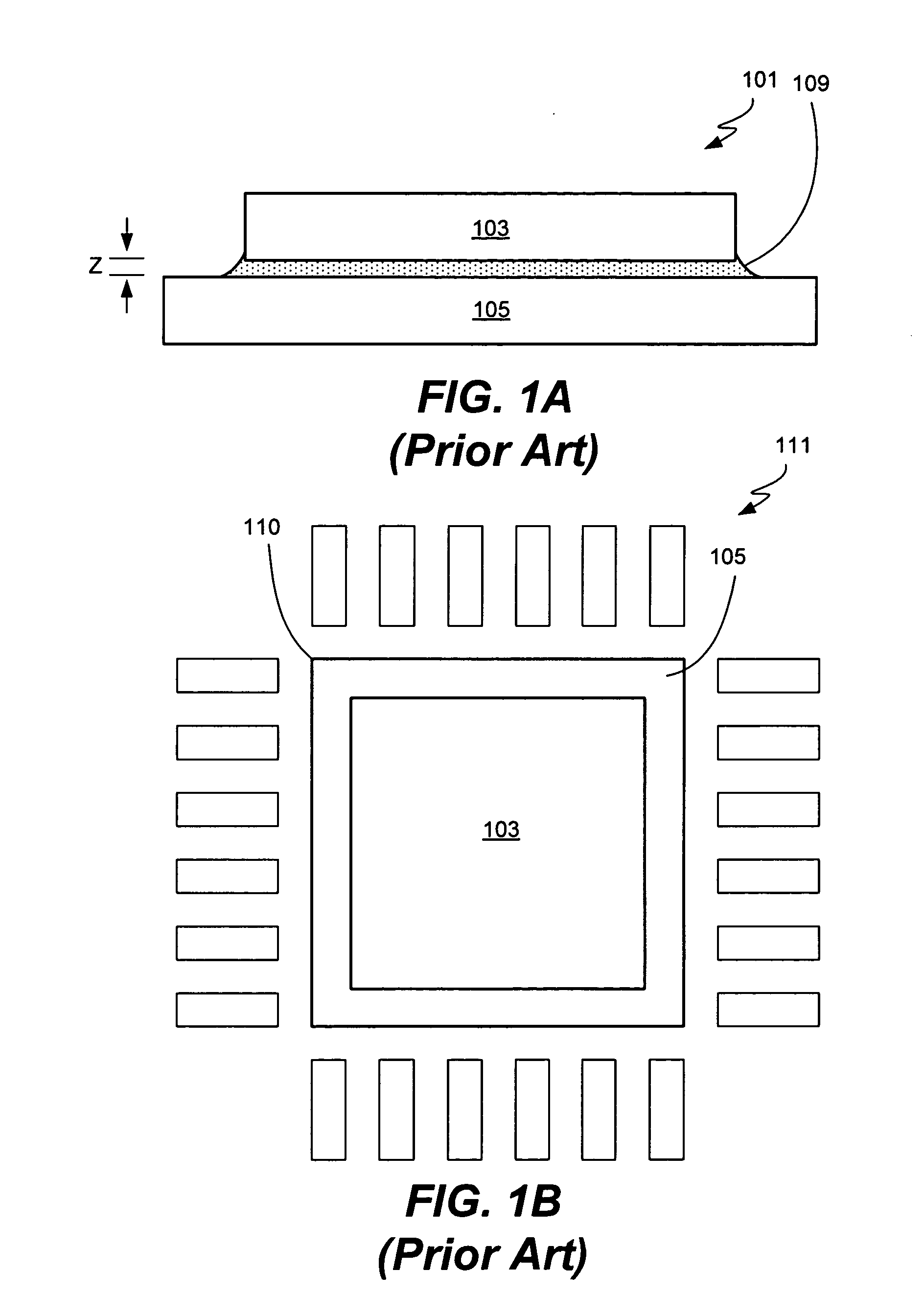
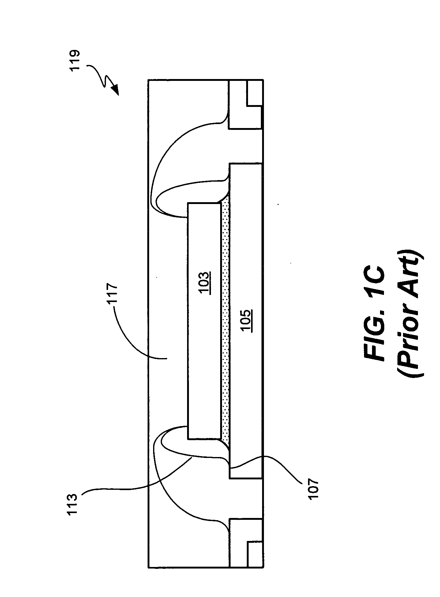
[0033]Referring next to FIGS. 2A-2C, an improved leadframe design in accordance with one aspect of the invention will be described. FIG. 2A is a diagrammatic top view of a leadframe strip suitable for use in packaging integrated circuits. Leadframe strip 201 is formed from a suitable conductive material. Typically the leadframe strip is formed from a metallic material such as copper, copper alloy, aluminum etc., although this is not a requirement. In the illustrated embodiment, the leadframe strip 201 has a number of ...


PUM


Abstract

One aspect of the invention pertains to a semiconductor package having a die and a die attach pad with a plurality of spaced apart pedestals supported by a web. A die is mounted on the die attach pad such that the die is supported by at least a plurality of the pedestals. Selected edge regions of the die are arranged to overlie recessed regions of the die attach pad between adjacent pedestals. The die is electrically connected to at least some of the contact leads. An adhesive is arranged to secure the die to the die attach pad, with the thickness of the adhesive between the web of the die attach pad and the die being greater than the thickness of the adhesive between the die and the top surfaces of the pedestals that support the die. The die attach pad may have rounded peripheral corners between adjacent edge surfaces of the die attach pad. In another aspect of the invention, a method of packaging integrated circuits is described, wherein the resulting packages include at least some of the aforementioned leadframe structures.

Description

BACKGROUND OF THE INVENTION[0001]The present invention relates generally to the packaging of integrated circuits (ICs). More particularly, a variety of leadframe designs suitable for use in packaging IC dice are described that facilitate stress reduction in and around an attached die.[0002]There are a number of conventional processes for packaging integrated circuit (IC) dice. By way of example, many IC packages utilize a metallic leadframe. The leadframe typically includes a plurality of leads or contacts, and optionally a die attach pad (paddle) upon which a die may be physically attached by means of a suitable adhesive material. The die is typically electrically connected to the leadframe leads by appropriate connectors such as bonding wires. In general, the die and portions of the leadframe are encapsulated with a molding material to protect the electrical connections and the delicate electrical components on the active side of the die.[0003]During testing and operation, package...

Claims


Application Information

Patent Timeline
IPC IPC(8): H01L23/495H01L21/56
CPCH01L23/3107H01L24/48H01L24/32H01L24/83H01L24/97H01L2224/27013H01L2224/32014H01L2224/32057H01L2224/32245H01L2224/48091H01L2224/48247H01L2224/48257H01L2224/73265H01L2224/83051H01L2224/83136H01L2224/83385H01L2224/8385H01L2224/92247H01L2224/97H01L2924/01013H01L2924/01027H01L2924/01029H01L2924/01082H01L2924/07802H01L2924/14H01L23/49503H01L2924/01006H01L2924/01033H01L2224/85385H01L2924/00014H01L2924/00H01L2924/3512H01L2924/181H01L2924/00012H01L2224/45099H01L2224/45015H01L2924/207
Inventor NGUYEN, LUU T.GUMASTE, VIJAYLAXMI
Owner NAT SEMICON CORP
Why Eureka
Try Eureka