Chip on film structure

a technology of film structure and chip, applied in the direction of circuit inspection/indentification, instruments, optics, etc., can solve the problems of reducing the reliability of the chip on the film structure, omitting the additional tape carrier package, and increasing the demand for display panel components

Active Publication Date: 2009-06-18
AU OPTRONICS CORP
View PDF6 Cites 22 Cited by
  • Summary
  • Abstract
  • Description
  • Claims
  • Application Information

AI Technical Summary

Benefits of technology

[0009]The embodiments of the invention provide a chip on film structure for a liquid crystal display. The chip on film structure includes a film substrate, a driver chip disposed on the film substrate, a plurality of input pads, and a plurality of output pads. The input pads and the output pads are disposed on two opposite si...

Problems solved by technology

Display panel demand and cost concerns have created a tendency to omit the additional tape carrier packages, for example, by directly bonding driver chips on the glass substrate (COG) or bonding driver chips on the film substrate (COF).
However, input pads and the output pads of the chip on film structure packaged with the driver chip may be cut when the chip on film structure is punched from the tape, and the metal particles may be generated.
T...

Method used


Image

  • Chip on film structure
  • Chip on film structure
  • Chip on film structure

Examples


Embodiment Construction

[0016]Reference will now be made in detail to the present preferred embodiments of the invention, examples of which are illustrated in the accompanying drawings. Wherever possible, the same reference numbers are used in the drawings and the description to refer to the same or like parts.

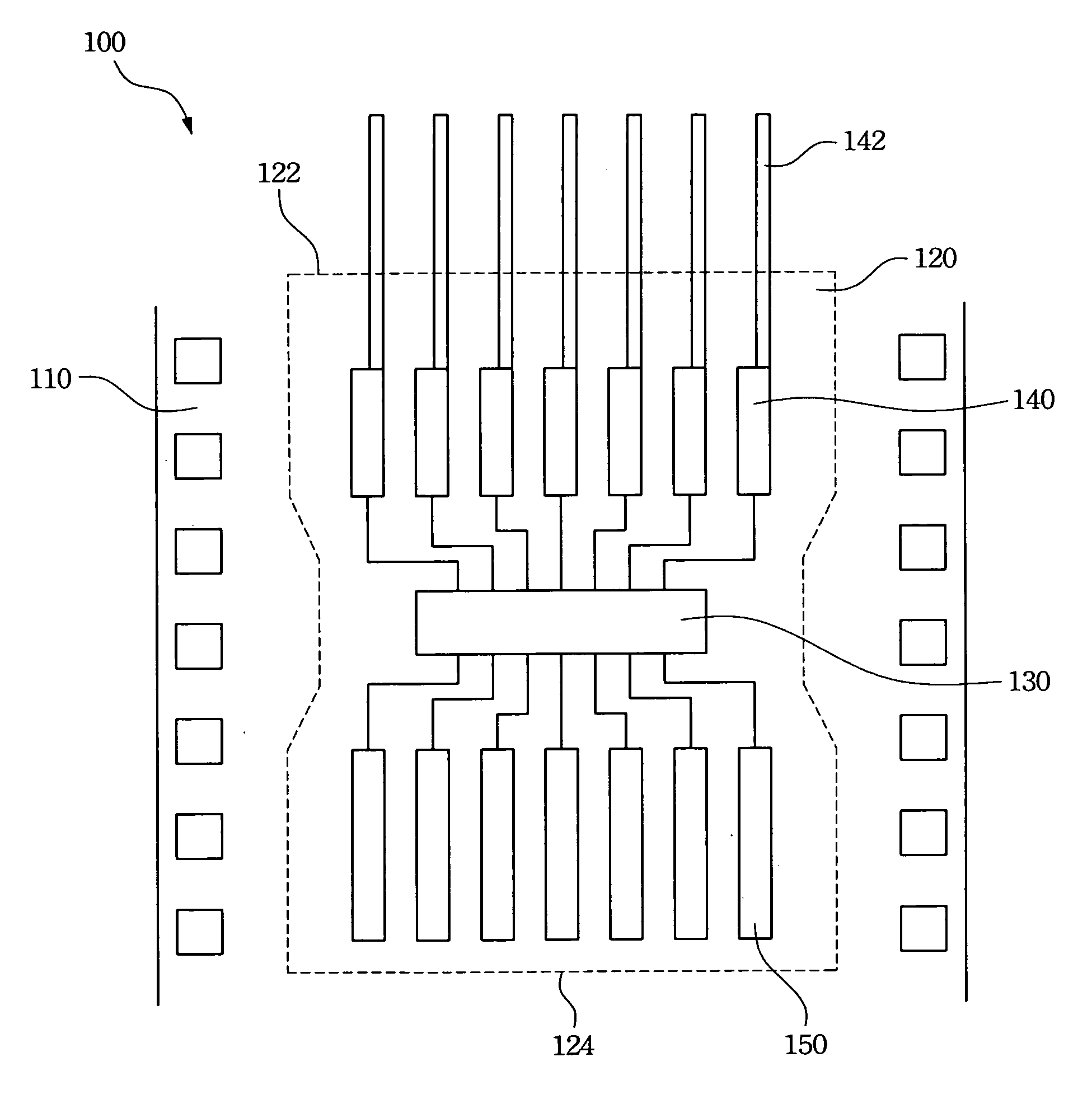
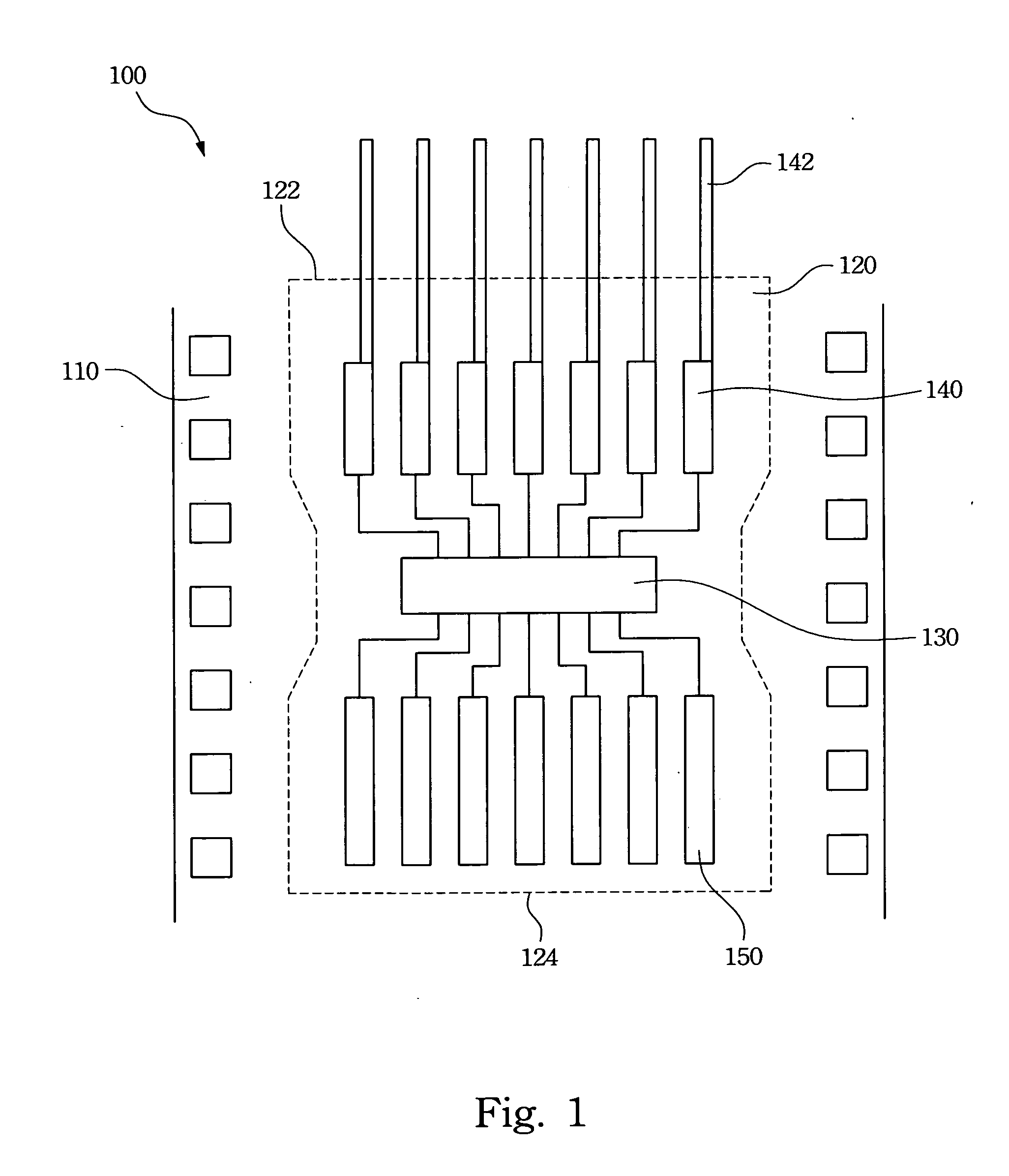
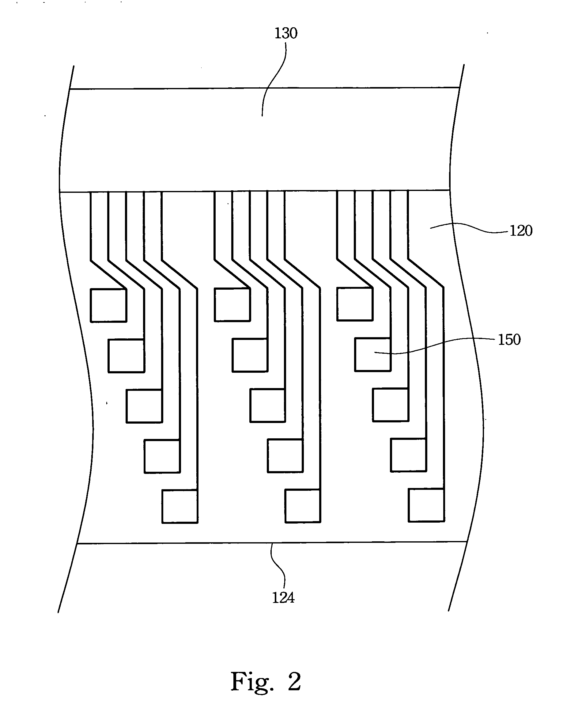
[0017]Refer to FIG. 1. FIG. 1 illustrates a schematic diagram of the chip on film (COF) structure of the invention. The chip on film structure 100 may be utilized in a liquid crystal display. The chip on film structure 100 includes a film substrate 120, a driver chip 130 disposed on the film substrate 120, a plurality of input pads 140, and a plurality of output pads 150. The driver chip 130 is electrically connected to both the input pads 140 and the output pads 150. The input pads 140 are electrically connect to a printed circuit board (not shown), which provides a signal source, and the output pads 150 are electrically connected to a glass panel (not shown). The image signal generated from the pri...


PUM


Abstract

The chip on film structure for a liquid crystal display is disclosed. The chip on film structure includes a film substrate, a driver chip disposed on the film substrate, a plurality of the input pad, and a plurality of output pads. The input pads and the output pads are disposed on two opposite sides of the driver chip, and are electrically connect to the driver chip respectively. Each input pad comprises an extending portion extending from the input pads to a first cutting edge respectively, and a width of the extending portion is thinner than a width of the input pad, and the extending portions are cut along the first cutting edge.

Description

RELATED APPLICATIONS[0001]This application claims priority to Taiwan Application Serial Number 96147529, filed Dec. 12, 2007, which is herein incorporated by reference.BACKGROUND[0002]1. Field of Invention[0003]The present invention relates to a chip on film structure. More particularly, the present invention relates to a chip on film structure for a liquid crystal display.[0004]2. Description of Related Art[0005]Recently, liquid crystal displays (LCD) have been widely applied in electrical products, due to the rapid progress of optical technology and semiconductor technology. Moreover, with the advantages of high image quality, compact size, light weight, low driving voltage, and low power consumption, LCDs have been introduced into portable computers, personal digital assistants, color televisions, and are gradually replacing the cathode ray tubes (CRT) used in conventional displays. LCDs have become the mainstream display apparatus.[0006]Conventional display panels have two types...

Claims


Application Information

Patent Timeline
IPC IPC(8): G02F1/1345
CPCG02F1/13452H01L23/4985H05K1/0268H05K1/0393H05K1/117H05K3/0052H05K3/361H01L2924/0002H05K2201/09727H05K2201/10681H05K2203/175H01L2924/00
Inventor CHANG, KE-CHIHYANG, CHIH-HSIANGHSU, SHENG-KAIHUANG, YI-CHIHCHEN, YING-CHAO
Owner AU OPTRONICS CORP
Why Eureka
Try Eureka