Correction method and exposure apparatus

a technology of exposure apparatus and correction method, which is applied in the field of correction method and exposure apparatus, can solve the problems of reducing the accuracy of overlay, and difficult to remove non-linear components by using ega wafer alignment, and achieves the effect of short time and effective correction of non-linear components

Active Publication Date: 2009-06-18
NIKON CORP
View PDF13 Cites 60 Cited by
  • Summary
  • Abstract
  • Description
  • Claims
  • Application Information

AI Technical Summary

Benefits of technology

[0014]According to the above-mentioned aspect, when the correction device has a plurality of correction functions that have different degree of non-linear components that can be considered, among the non-linear components of the two-dimensional grid, which is a reference for the position where each of the divided areas is formed on the photosensitive object loaded into the transfer device, it is possible to select at least one optimum correction function, on the basis of predetermined information associated with at least one of the transfer device and the photosensitive object loaded into the transfer device. Therefore, when a plurality of divided areas are formed on the photosensitive object loaded into the transfer device, it is possible to effectively correct non-linear components of a two-dimensional grid, which is a reference for the position where each of the divided areas is formed, in a short time.

Problems solved by technology

When the overlay exposure is performed using a plurality of exposure apparatuses, an error between the stage grids of the exposure apparatuses (an error between stage coordinate systems for defining the movement position of the wafer in each exposure apparatus) may occur, which is a factor causing a reduction in the overlay accuracy.
The distortion may cause a reduction in the overlay accuracy.
However, when non-linear components of the grid cannot be negligible, it is difficult to remove the non-linear components by using the EGA wafer alignment.

Method used


Image

  • Correction method and exposure apparatus
  • Correction method and exposure apparatus
  • Correction method and exposure apparatus

Examples


Embodiment Construction

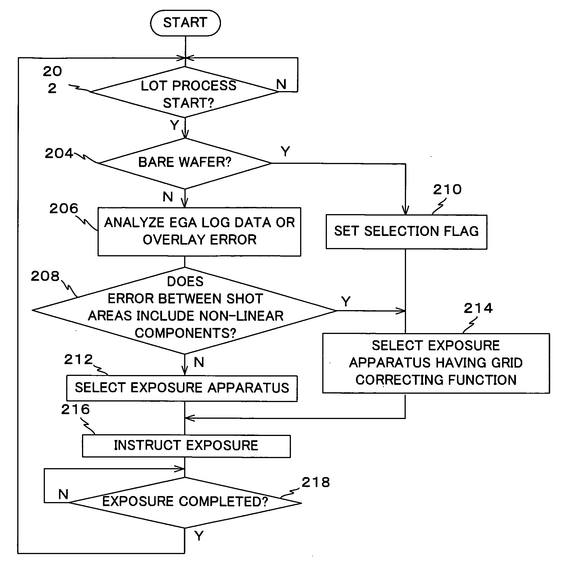
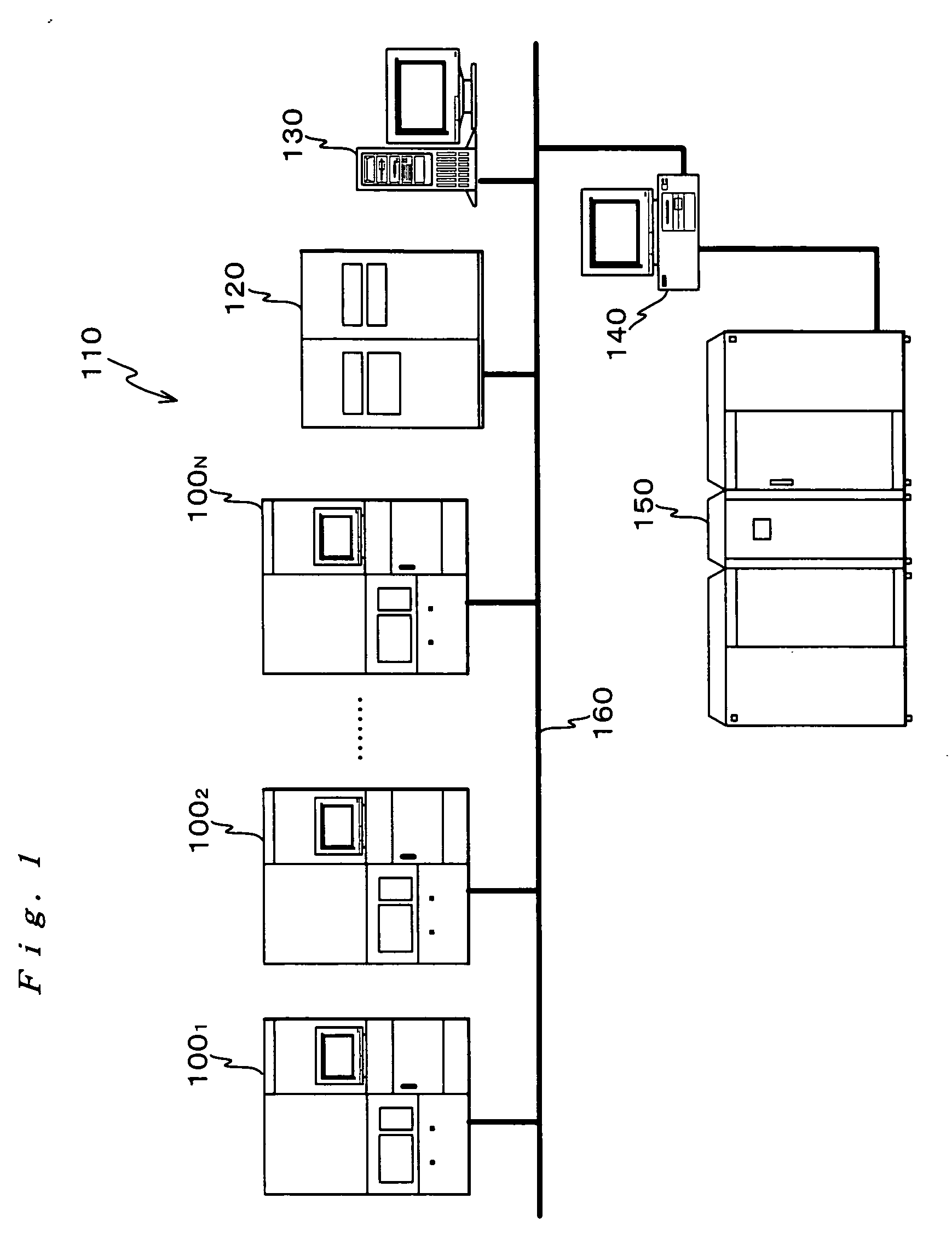
[0027]FIG. 1 is a diagram schematically illustrating the overall structure of a lithography system 110 according to an embodiment of the invention. The lithography system 110 is provided as a portion of a microdevice manufacturing line to perform a lithography process on a plurality of wafers, which are bases of the microdevices. In the lithography system 110, a plurality of wafers are managed in a predetermined processing unit, which is called a lot (for example, one lot is composed of 25 wafers), and the lithography process is performed on each lot of wafers.

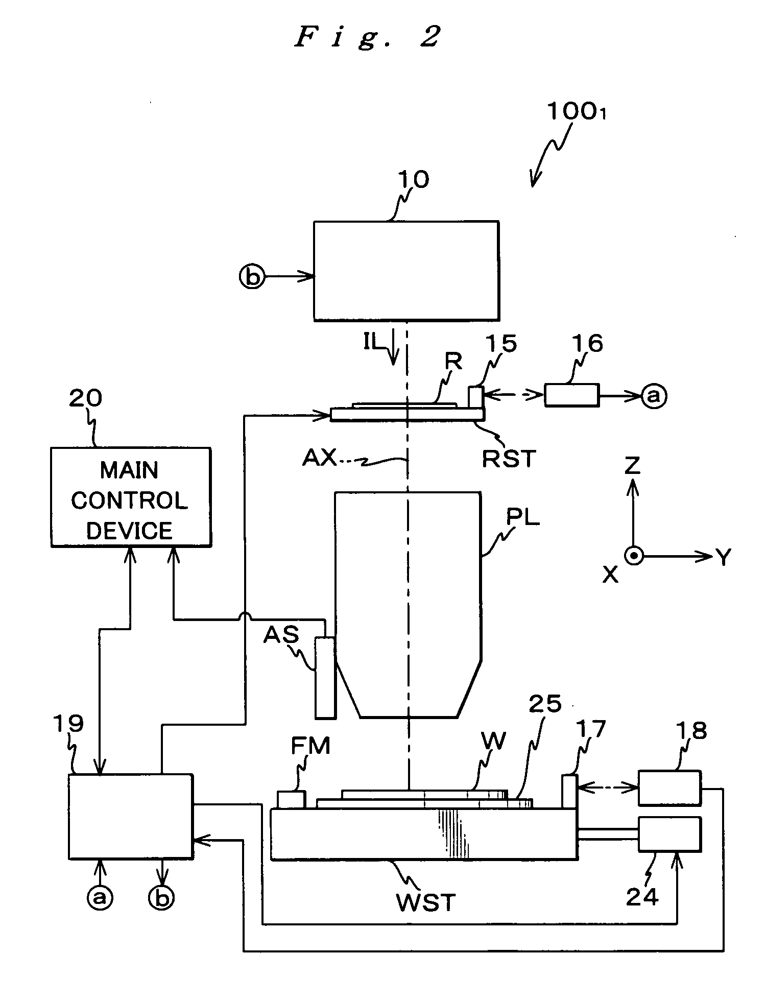
[0028]The lithography system 110 includes N exposure apparatuses 1001, 1002, . . . , 100N, a overlay measuring instrument 120, a central information server 130, a terminal server 140, a host computer 150 and the like. The exposure apparatuses 1001 to 100N, the overlay measuring instrument 120, the central information server 130, and the terminal server 140 are connected to one another through a local area network (LAN) 160. Th...


PUM


Abstract

At Step 602, the grid of a wafer loaded into an exposure apparatus is approximated by a mathematical function fitting up to, for example, a cubic function, and at Step 612, the magnitude of a residual error between the position of a sample shot area obtained by the function and an actually measured position is compared with a predetermined threshold value. GCM measurement is performed in a mathematical function mode in a subroutine 616, or it is performed in a map mode in a subroutine 616, on the basis of the result of the comparison. In addition, it is determined whether to extract non-linear components from the wafer in each lot on the basis of a variation in the temperature of the wafer (Step 622) and a variation in random error between the wafers (Step 624).

Description

TECHNICAL FIELD[0001]The present invention relates to a correction method and an exposure apparatus, and more particularly, to a correction method of, when a plurality of divided areas are formed by pattern transfer on each of a plurality of photosensitive objects sequentially loaded into an exposure apparatus, correcting the position of each of the photosensitive objects and to an exposure apparatus for forming by pattern transfer a plurality of divided areas on each of a plurality of photosensitive objects.BACKGROUND ART[0002]In order to prevent a reduction in yield in a manufacturing line of microdevices, such as semiconductor devices, it is necessary to keep the interlayer overlay accuracy of overlay exposure at a high level by overlaying circuit patterns or the like in several layers onto a substrate such as a wafer or the like (hereinafter, referred to as a wafer), to form by pattern transfer shot areas in a lithography process.[0003]When the overlay exposure is performed usin...

Claims


Application Information

Patent Timeline
Patent Type & Authority Applications(United States)
IPC IPC(8): G03B27/42G01B11/00
CPCG03F9/7003G03F7/70633
Inventor KAWAKUBO, MASAHARU
Owner NIKON CORP
Why Eureka
Try Eureka