

Semiconductor device including a plurality of cells
- Summary
- Abstract
- Description
- Claims
- Application Information
AI Technical Summary
Benefits of technology
Problems solved by technology
Method used
Image

Examples
Embodiment Construction
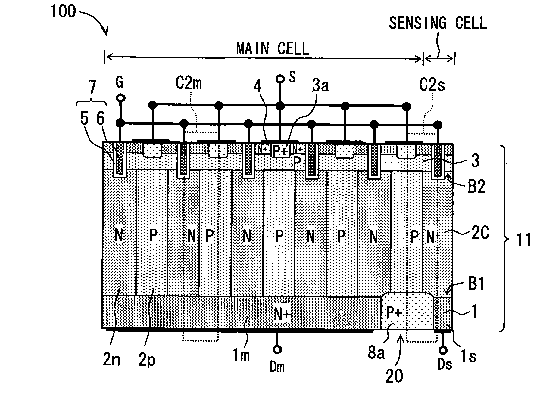
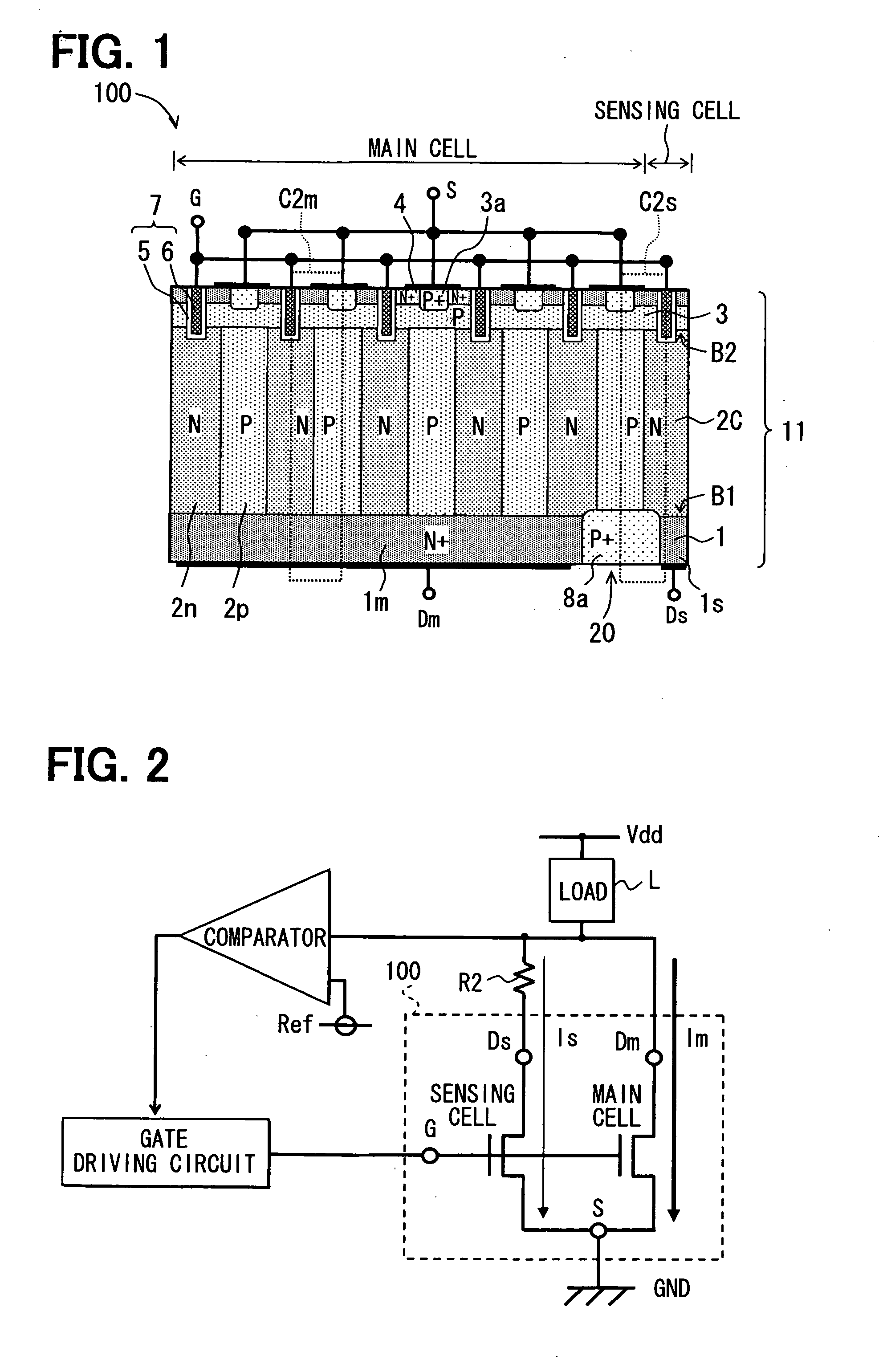
[0027]A semiconductor device 100 according to an exemplary embodiment of the invention will be described with reference to FIG. 1. The semiconductor device 100 includes an N channel power MOSFET made of an aggregation of a plurality of cells. Each of the cells is formed as a configurational repeating unit and has a diffusion structure similar to each other. The cells include a plurality of main cells C2m and at least one sensing cell C2s. The main cells C1m are provided for supplying an electric current to a load. The sensing cell C1s is provided for detecting a main current Im that flows in the main cells C2m. The number of the main cells C2m is larger than the number of the sensing cells C2s.
[0028]The semiconductor device 100 includes a semiconductor substrate 11. In the semiconductor substrate 11, P type columns 2p and N type columns 2n are alternately arranged in a direction approximately perpendicular to a thickness direction of the semiconductor substrate 11, for configurate ...
PUM
 Abstract
Description
Claims
Application Information