Electro-optic device, and TFT substrate for current control and method for manufacturing the same

a technology of current control and optical devices, applied in the direction of electrical devices, semiconductor devices, instruments, etc., can solve the problems of uneven luminance, lapse, and change in the amount of current flown in the organic el display device for each pixel, and achieve the effect of connecting to the pad

Inactive Publication Date: 2009-06-25
IDEMITSU KOSAN CO LTD
View PDF18 Cites 105 Cited by
  • Summary
  • Abstract
  • Description
  • Claims
  • Application Information

AI Technical Summary

Benefits of technology

[0100]By doing this, the pad for a data line, the pad for a scanning line, the pad for a measuring line, the pad for a capacitor line and the pad for an EL-driving line are formed immediately below the protective insulting film. As a result, connectability to the pad for a data line, the pad for a scanning line, the pad for a measuring line, the pad for a capacitor line and the pad for an EL-driving line can be improved.

Problems solved by technology

However, variations in the properties of the driving transistor results in a change in the amount of current flown in an organic EL display device for each pixel.
In such a case, unevenness in luminance occurs.
However, luminance decreases with the lapse of time when emission is performed continuously.

Method used


Image

  • Electro-optic device, and TFT substrate for current control and method for manufacturing the same
  • Electro-optic device, and TFT substrate for current control and method for manufacturing the same
  • Electro-optic device, and TFT substrate for current control and method for manufacturing the same

Examples


first embodiment

of a TFT Substrate for Current Control

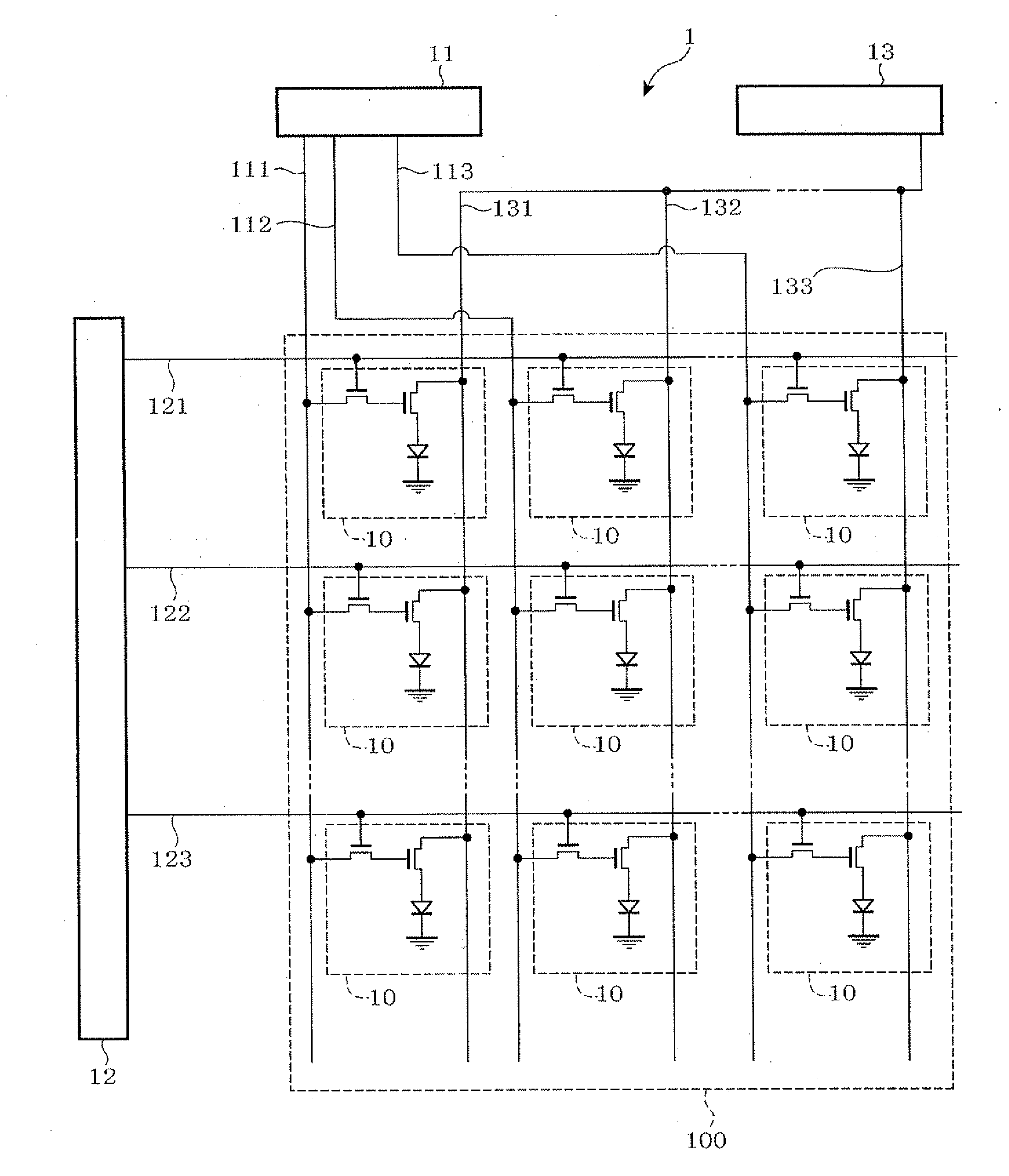
[0235]As shown in FIG. 1, in the TFT substrate 100 of this embodiment, m (row; m is a natural number)×n (line; n is a natural number) pixels 10 are arranged in a matrix on a glass substrate 101.

[0236]Furthermore, in the direction of line (horizontal direction), n pieces of the scanning lines 121, 122, . . . 123 are formed. For example, the nth scanning line 123 is connected in parallel with m pieces of the pixel 10 arranged in the nth line.

[0237]In addition, in the direction of row (vertical direction), m pieces of the data lines 111, 112, . . . 113 are formed. For example, the mth data line 113 is connected in parallel with n pieces of pixel 10 arranged in the mth row.

[0238]Furthermore, in the direction of row (vertical direction), m pieces of the scanning lines 131, 132, . . . 133 are formed. For example, the mth EL-driving line 133 is connected in parallel with n pieces of pixel 10 arranged in the mth row.

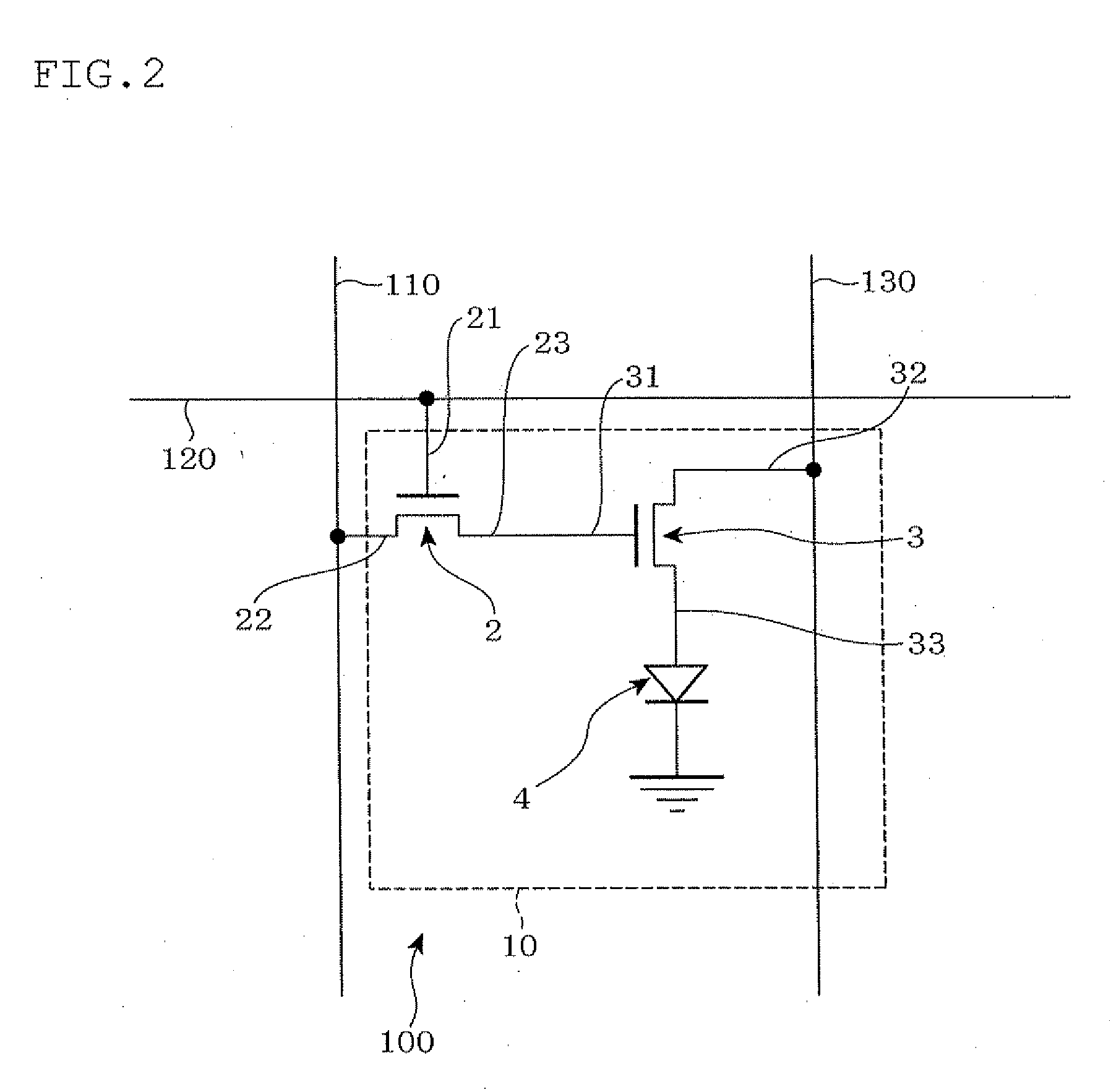
[0239]As shown in FIG. 13, each pixel...

second embodiment

of a TFT Substrate for Current Control

[0347]As shown in FIG. 17, in the TFT substrate 100 of this embodiment, m (row; m is a natural number)×n (line; n is a natural number) pixels 10a are arranged in a matrix.

[0348]Furthermore, in the direction of line (horizontal direction), n pieces of the scanning lines 121, 122, . . . 123 are formed. For example, the nth scanning line 123 is connected in parallel with m pieces of the pixel 10a arranged in the nth line.

[0349]In addition, in the direction of line (horizontal direction), n pieces of the EL-driving lines 131a, 132a, . . . 133a are formed. For example, the nth EL-driving line 133a is connected in parallel with m pieces of pixel 10a arranged in the nth line.

[0350]In addition, in the direction of row (vertical direction), m pieces of the data lines 111, 112, . . . 113 are formed. For example, the mth data line 133 is connected in parallel with n pieces of pixel 10a arranged in the mth row.

[0351]Furthermore, in the direction of row (ver...

third embodiment

of a TFT Substrate for Current Control

[0483]As shown in FIG. 39, in the TFT substrate 100c of this embodiment, m (row; m is a natural number)×n (line; n is a natural number) pixels 10c are arranged in a matrix on the glass substrate 101.

[0484]Furthermore, in the direction of line (horizontal direction), n pieces of the scanning lines 121, 122, . . . 123 are formed. For example, the nth scanning line 123 is connected in parallel with m pieces of the pixel 10c arranged in the nth line.

[0485]In addition, in the direction of line (horizontal direction), n pieces of the EL-driving lines 131a, 132a, . . . 133a are formed. For example, the nth EL-driving line 133a is connected in parallel with m pieces of pixel 10c arranged in the nth line.

[0486]In addition, in the direction of line (horizontal direction), n pieces of the capacitor lines 160 are formed. For example, the nth capacitor line 160 is connected in parallel with m pieces of pixel 10c arranged in the nth line.

[0487]In addition, in...


PUM


Abstract

To provide an electro-optic apparatus which can directly control alternating current, output significantly high-frequency alternating current, stably output a large amount of power, and reduce manufacturing cost, as well as a TFT substrate for current control and the method for producing the same.
A dispersion-type inorganic EL display apparatus 1c as an electro-optic apparatus is provided with a data line-driving circuit 11, a scanning line-driving circuit 12, a power supply line-controlling circuit 13a, a current-measuring circuit 15 and a TFT substrate 100c.

Description

TECHNICAL FIELD[0001]The invention relates to an electro-optic apparatus, a TFT substrate for current control and a method for producing the same. In particular, according to the electro-optic apparatus, the TFT substrate for current control and the method for producing the same of the invention, alternating current can be directly controlled, significantly high-frequency alternating current can be output, a large amount of current can be output stably, and manufacturing cost can be reduced.BACKGROUND[0002]An organic EL display apparatus has attracted attention as a next-generation display or solid illumination replacing an LCD (Liquid Crystal Display). The reason therefor is as follows. Since an organic EL (Electronic Luminescence) device is a self-emitting device, it has less dependency on viewing angle. In addition, an organic EL display device has excellent properties such as lower power consumption since no backlight or reflected light is needed.[0003]As the method for driving ...

Claims


Application Information

Patent Timeline
Patent Type & Authority Applications(United States)
IPC IPC(8): G09G3/30H01L21/30
CPCG09G3/3233G09G2300/0417G09G2300/0842G09G2300/0852G09G2320/029G09G2320/0295G09G2320/043H01L27/1214H01L27/1225H01L29/7869H01L27/1255H01L27/1288H01L29/45H01L27/124H10K59/131
Inventor INOUE, KAZUYOSHIYANO, KOKITANAKA, NOBUOTANAKA, TOKIE
Owner IDEMITSU KOSAN CO LTD
Why Eureka
Try Eureka