Semiconductor memory input/output device

a technology of semiconductor memory and input/output device, which is applied in the direction of information storage, static storage, digital storage, etc., can solve the problems of deteriorating operation characteristics of semiconductor memory devices, becoming very difficult to dispose lines in semiconductor memory devices, etc., and achieve the effect of reducing the overall size of semiconductor memory devices

Active Publication Date: 2009-06-25
SK HYNIX INC
View PDF3 Cites 15 Cited by
  • Summary
  • Abstract
  • Description
  • Claims
  • Application Information

AI Technical Summary

Benefits of technology

[0019]Embodiments of the present invention are directed to providing a semiconductor memory input/output device for reducing an overal...

Problems solved by technology

Since lines and pads must not be overlapped, it becomes very difficult to dispose lines in a semiconductor memory ...

Method used


Image

  • Semiconductor memory input/output device
  • Semiconductor memory input/output device
  • Semiconductor memory input/output device

Examples


Embodiment Construction

[0038]Other objects and advantages of the present invention can be understood by the following description, and become apparent with reference to the embodiments of the present invention.

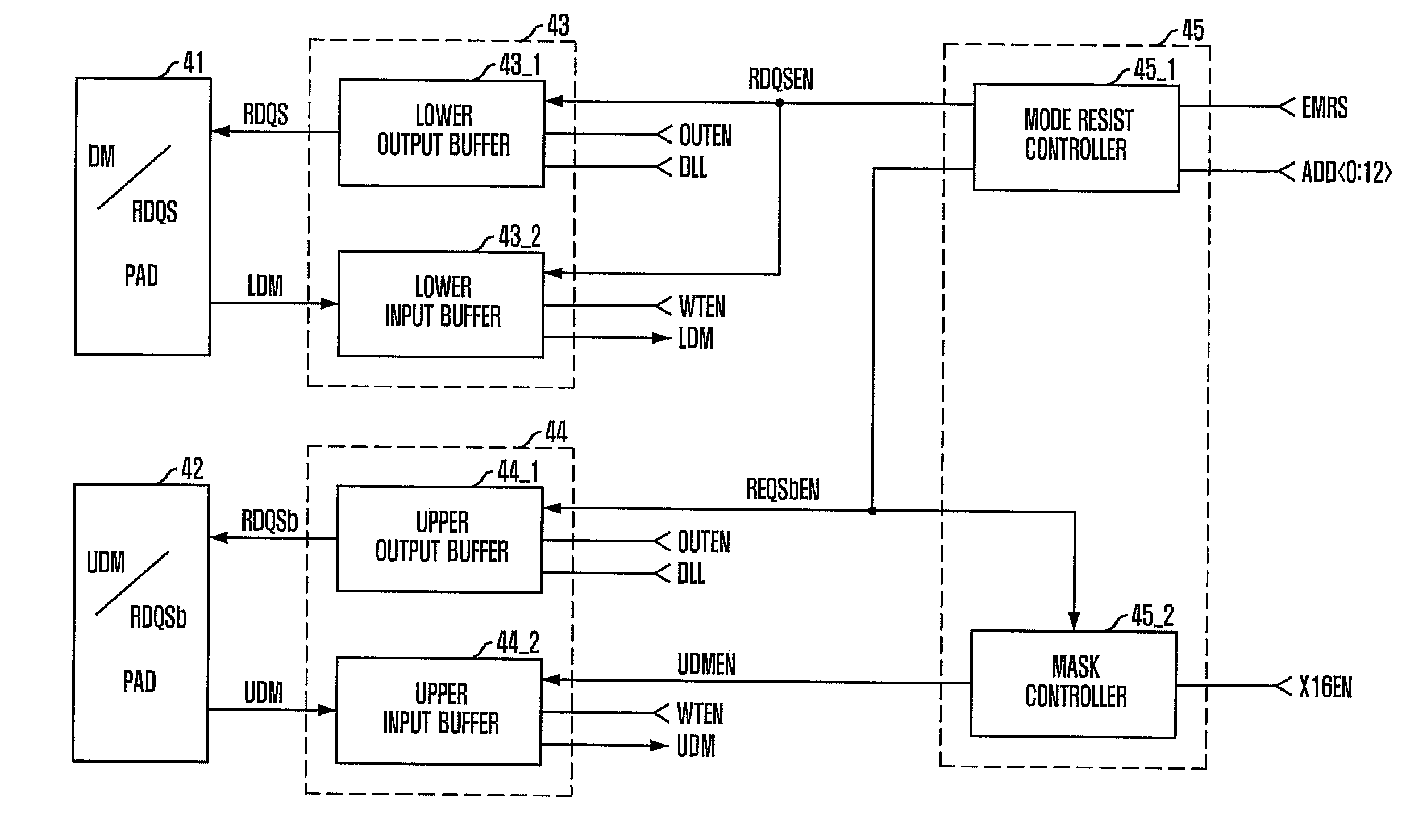
[0039]The present invention relates to a semiconductor memory input / output device for reducing the number of pads in a semiconductor memory device supporting a multi-operation mode by sharing pads for signals that are independently used in each of operation modes.

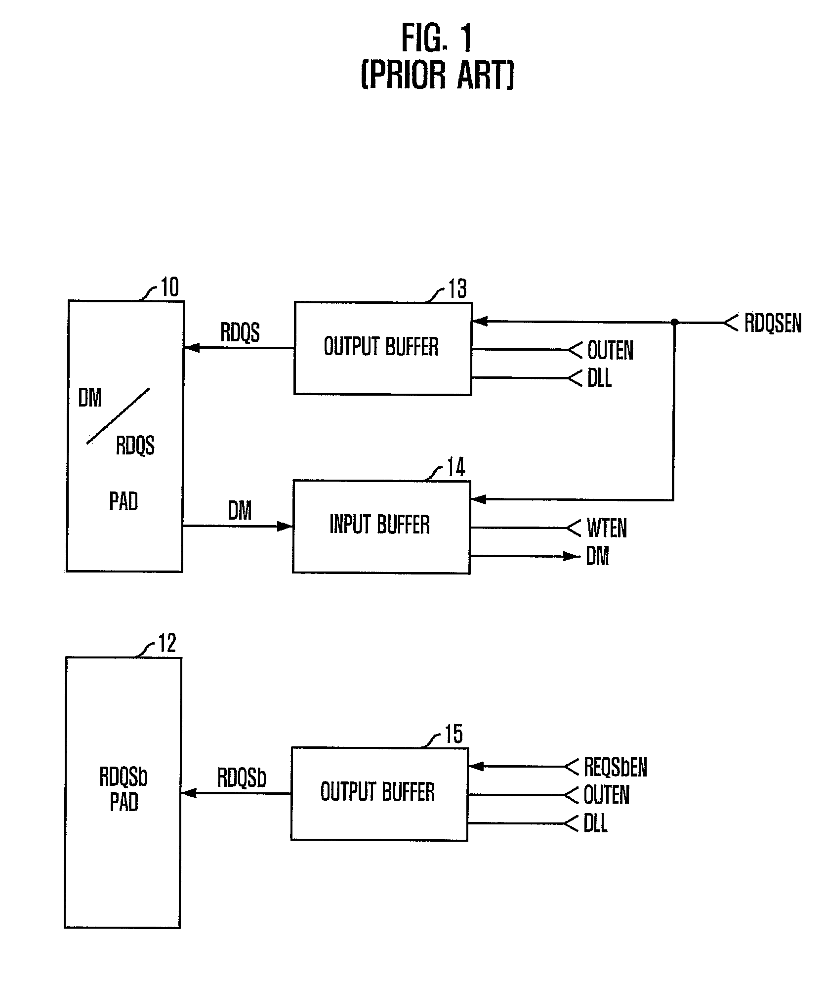
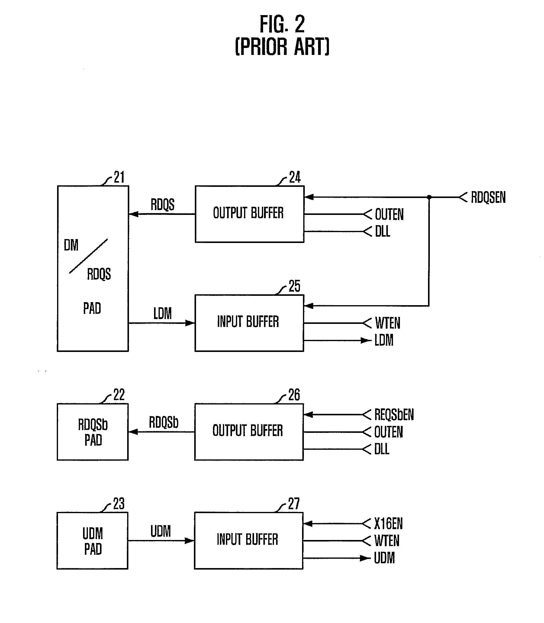
[0040]The present invention relates to sharing pads for a read data strobe signal RDQS and a data mask signal DM by setting an extended mode register set when a semiconductor memory device operates in an X8 operation mode defined in the DDR2 SDRAM specification.

[0041]That is, the number of pads in a semiconductor memory device supporting a multi-operation mode is reduced by sharing one pad for both of an inverted read data strobe signal RDQSb of the X8 operation mode and an upper data mask signal UDM for the X16 operation mode.

[0042]Accordi...


PUM


Abstract

A semiconductor memory input/output device includes selection pads used to input and output signals for multiple operation modes and having multiple functions, a control signal generator for outputting setting signals and a mask control signal, a lower input/output unit including a lower output buffer for outputting a read data strobe signal to a selection pad and a lower input buffer for receiving a lower data mask signal from the selection pad, and selecting one operation of the lower output buffer and the lower input buffer, and an upper input/output unit including an upper output buffer for outputting an inverted read data strobe signal to the second selection pad and an upper input buffer for receiving an upper data mask signal from the second selection pad, and selecting one operation of the upper output buffer and the upper input buffer.

Description

CROSS-REFERENCE TO RELATED APPLICATION[0001]The present invention claims priority of Korean patent application number 10-2007-0134661, filed on Dec. 20, 2007, which is incorporated by reference in its entirety.BACKGROUND OF THE INVENTION[0002]The present invention relates to a semiconductor memory device, and more particularly, to a semiconductor memory input / output device supporting a multi-operation mode.[0003]In order to increase an operating speed of a semiconductor memory device, recent semiconductor technology continuously increases an operating frequency. Additionally, the number of data bits simultaneously inputted to or outputted from the semiconductor memory device increases. As a result, recent semiconductor memory devices include an increased number of pads for inputting and outputting data.[0004]For example, a semiconductor memory device supporting an X8 operation mode includes eight data pads for inputting and outputting 8-bit data at the same time, two data strobe pad...

Claims


Application Information

Patent Timeline
IPC IPC(8): G11C7/10
CPCG11C7/1045G11C7/1051G11C7/1057G11C7/22G11C7/1078G11C7/1084G11C7/1093G11C7/1066G11C7/10
Inventor HA, SUNG-JOOCHO, HO-YOUB
Owner SK HYNIX INC
Why Eureka
Try Eureka