Light-emitting device with inorganic housing

Active Publication Date: 2009-07-02
SIGNIFY HLDG BV
View PDF6 Cites 12 Cited by
  • Summary
  • Abstract
  • Description
  • Claims
  • Application Information

AI Technical Summary

Benefits of technology

[0028]One advantage with the method is that the contact layer can be arranged in the recess at high temperature, preferably at a temperature where the contact layer material is in a liquid state to easily spread in the recess, and to allow a good con

Problems solved by technology

Light extraction is a key issue for light emitting devices.
A common problem with semiconductor light-emitting devices is that the efficiency with which light may be extracted from the device is reduced due to internal reflection in the interface between the device and the surroundings, followed by reabsorption of the reflected light in the device.
However, in high power applications, where single solid-state light emitting devices with an effect of up to 3 Watts per square

Method used


Image

  • Light-emitting device with inorganic housing
  • Light-emitting device with inorganic housing
  • Light-emitting device with inorganic housing

Examples


Embodiment Construction

[0032]The present invention will now be described more in detail with reference to the drawings.

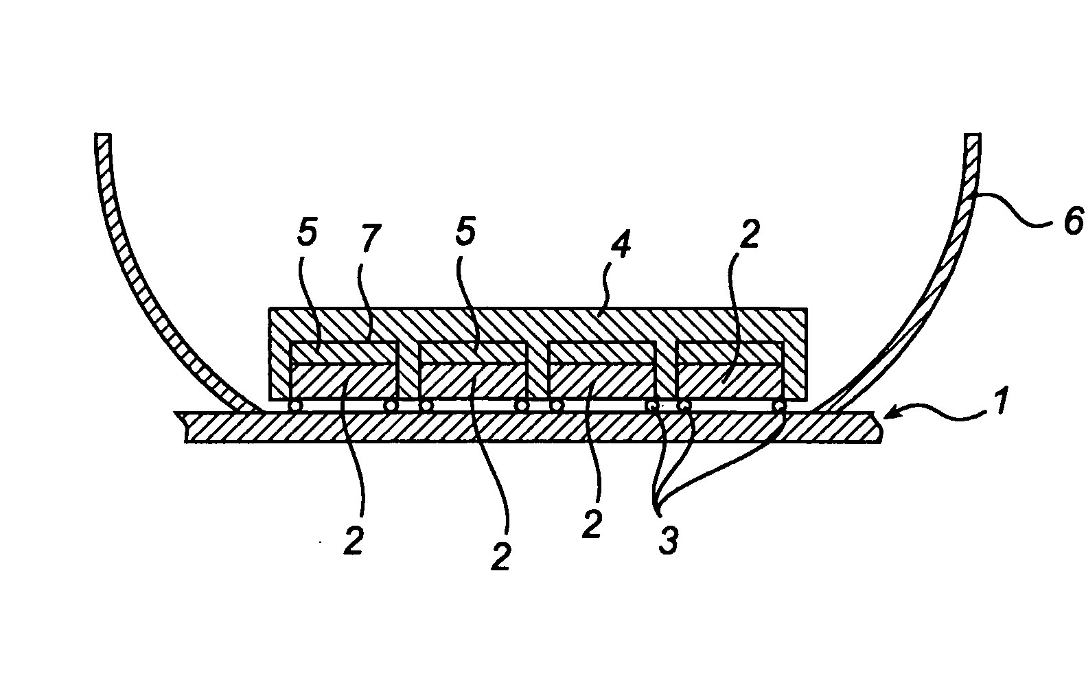
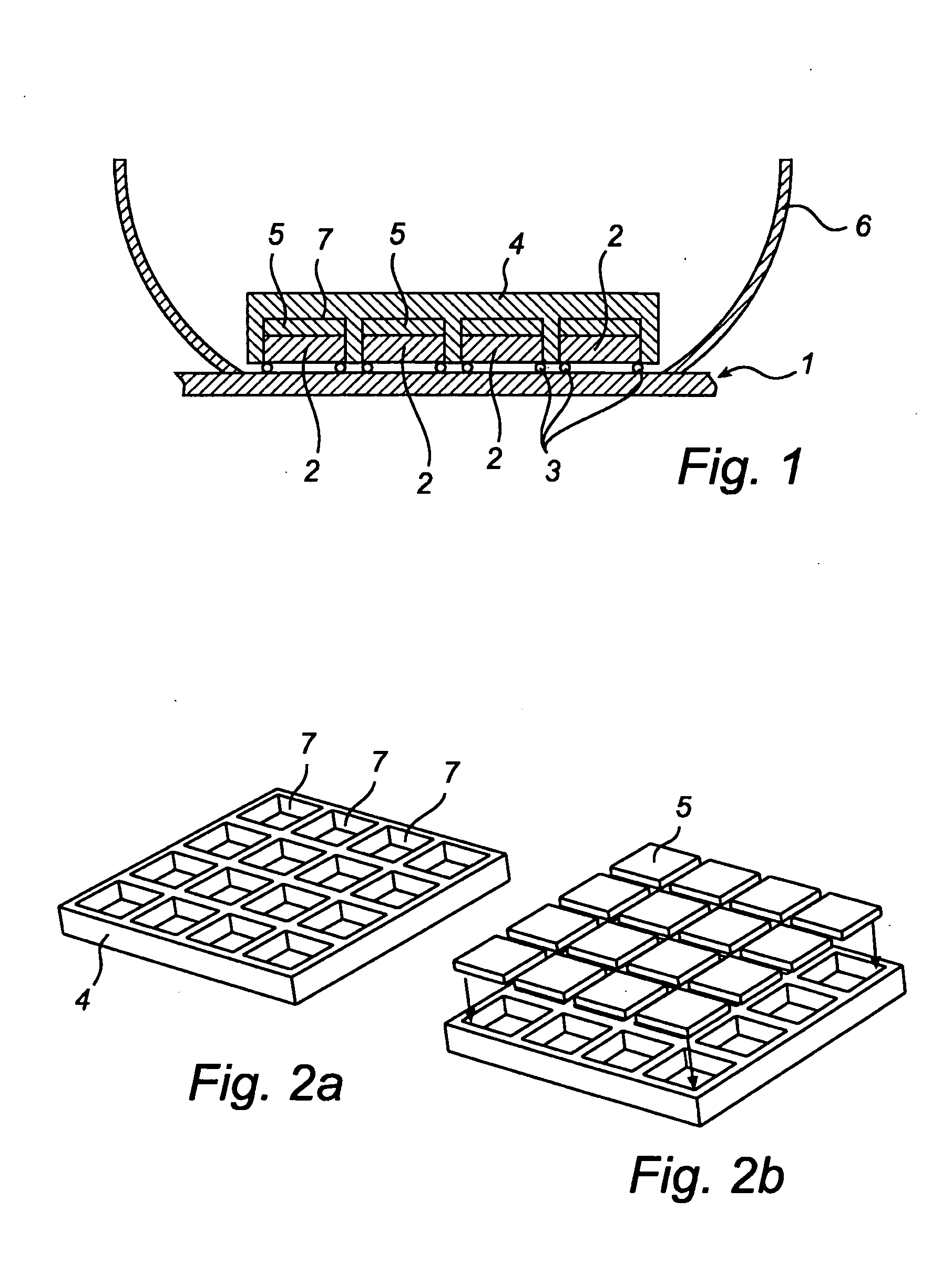
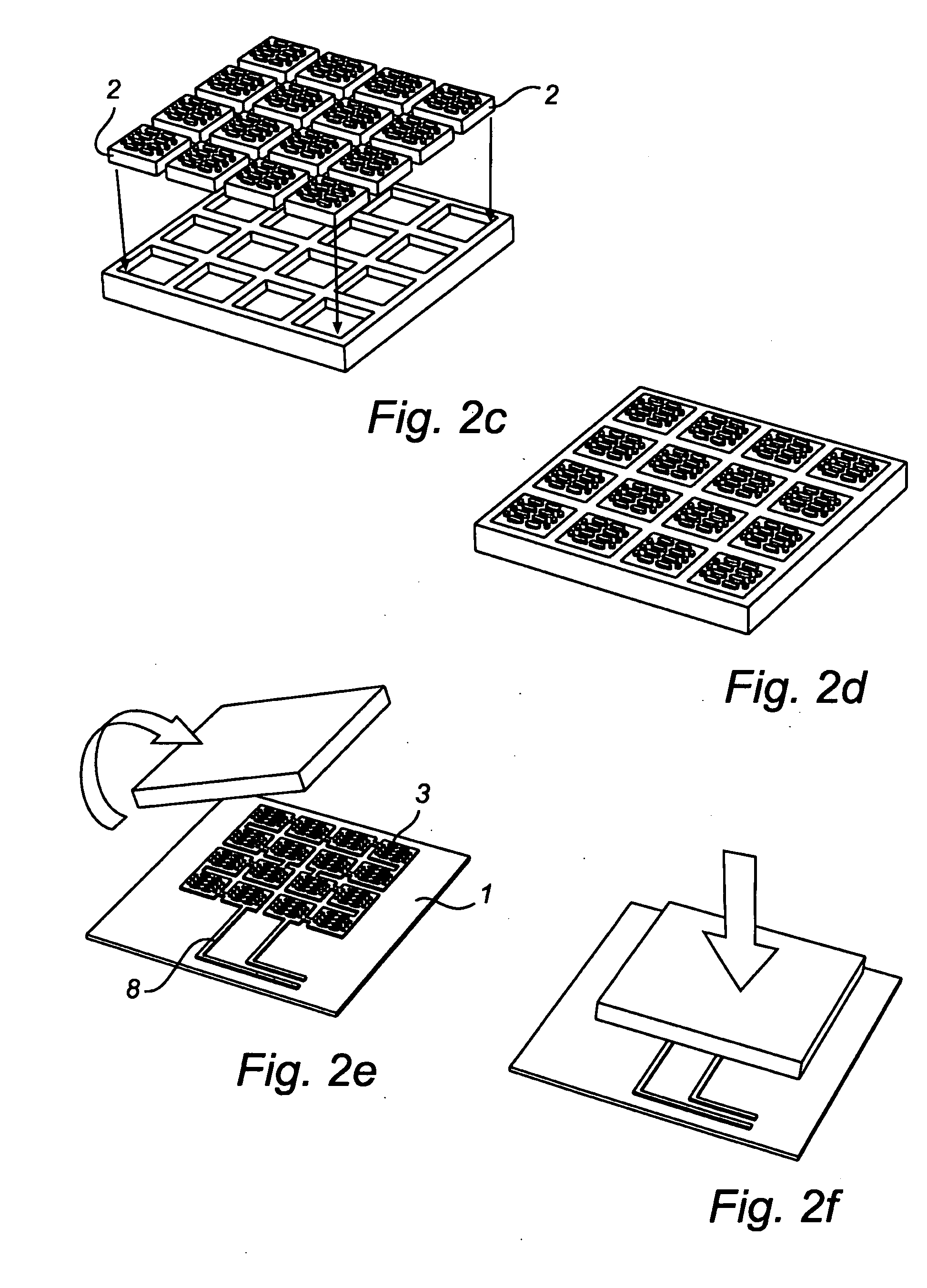
[0033]A preferred embodiment of the present invention, as shown in FIG. 1, comprises a substrate 1 provided with a circuitry. An array of light-emitting diodes (LEDs) 2 are arranged on the circuitry, and each LED of the array are separately connected to the circuitry by metal bumps 3 at pre-determined positions.

[0034]The LEDs 2 are arranged in separate recesses in a housing 4 of a translucent inorganic material, and the location and the orientation of each LED is determined by the walls of the recess. A translucent inorganic contact layer 5 is arranged between each LED and the housing 4, in the recesses to optically connect and physically bind the LED to the housing.

[0035]Furthermore, a specular reflector 6 is arranged on the substrate 1 to collimate the light emitted by the device.

[0036]A preferred method for the manufacture of a light-emitting device of the present invention is outlined...


PUM


Abstract

The present invention relates to a light-emitting device comprising at least one light-emitting diode, which emits light, and a housing arranged to receive at least a portion of said light. The housing comprises a translucent inorganic material and is provided with at least one recess, which comprises positioning and orientating means. The at least one light-emitting diode is arranged in the at least one recess and is positioned and orientated by said positioning and orientating means, and a translucent inorganic contact layer material is arranged between the at least one light-emitting diode and the housing in the at least one recess to receive at least portion of the light and to connect said light-emitting diode to said housing.

Description

TECHNICAL FIELD[0001]The present invention relates to a light-emitting device comprising a light-emitting diode, which emits light, and a housing arranged to receive at least a portion of said light. The invention also relates to methods for the manufacture of such light-emitting devices.TECHNICAL BACKGROUND[0002]Semiconductor light-emitting devices, such as light-emitting diodes (LEDs) and laser diodes (LDs), are among the most efficient and robust light sources currently available.[0003]Light extraction is a key issue for light emitting devices. A common problem with semiconductor light-emitting devices is that the efficiency with which light may be extracted from the device is reduced due to internal reflection in the interface between the device and the surroundings, followed by reabsorption of the reflected light in the device. The internal reflection is due to that the refractive index of the device materials is higher than the refractive index of the material in which the dev...

Claims


Application Information

Patent Timeline
IPC IPC(8): H01L33/00H01L21/50F21K99/00
CPCF21K9/00H01L25/0753H01L51/5237H01L51/5271H01L2924/0002H01L2251/5315H01L2924/00H01L25/075H10K50/84H10K50/856H10K2102/3026
Inventor BECKERS, LUCAS JOHANNES ANNA MARIA
Owner SIGNIFY HLDG BV
Why Eureka
Try Eureka