

Apparatus and method for data interface of flat panel display device
a flat panel display device and data interface technology, applied in the field of flat panel display devices, can solve the problems of increasing the amount of data transfer, unstable operation of the flat panel display device, and increasing electromagnetic interference (emi), so as to reduce the number of transfer lines and accurately sample data
- Summary
- Abstract
- Description
- Claims
- Application Information
AI Technical Summary
Benefits of technology
Problems solved by technology
Method used
Image

Examples
first embodiment
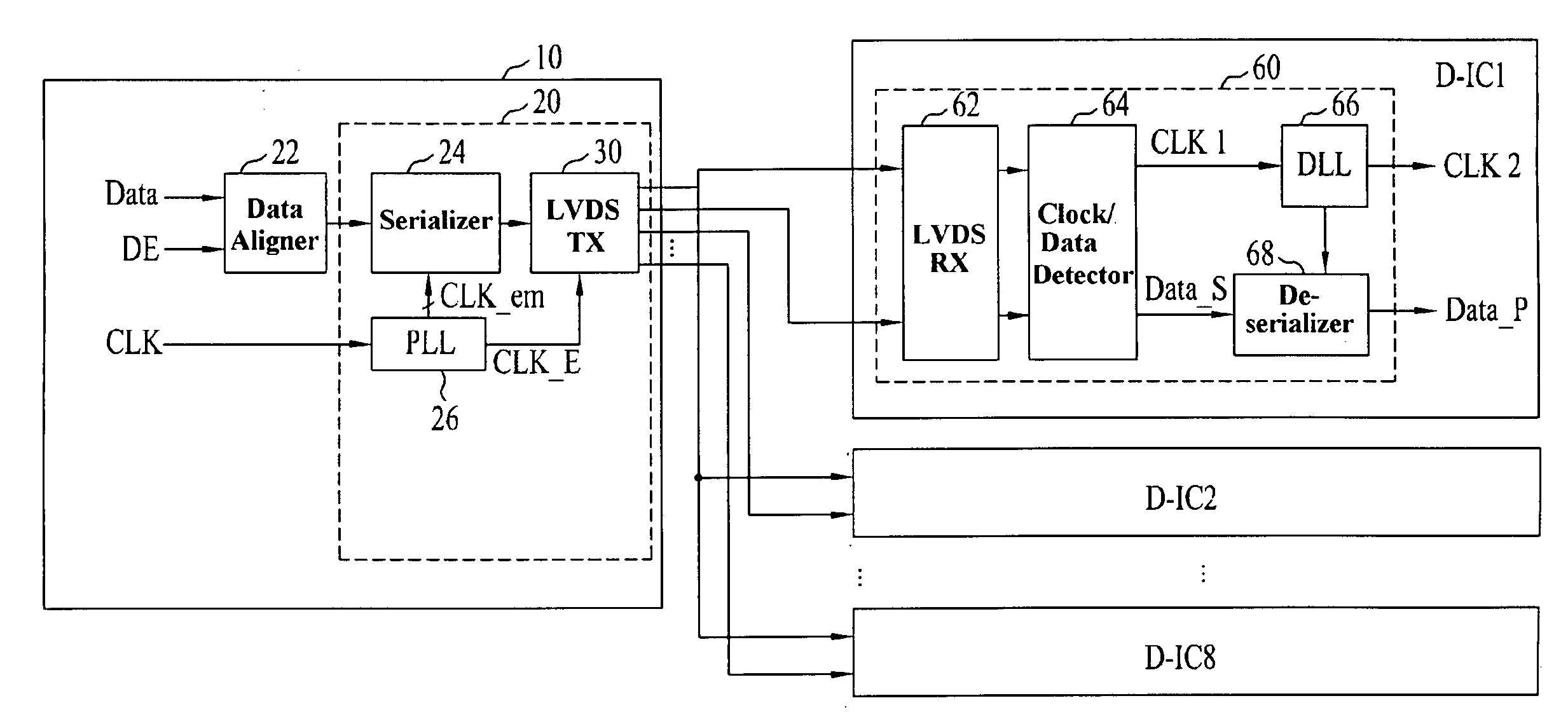
[0049]FIG. 1 is a block diagram schematically illustrating an apparatus for data interface of a flat panel display device in accordance with the present invention.
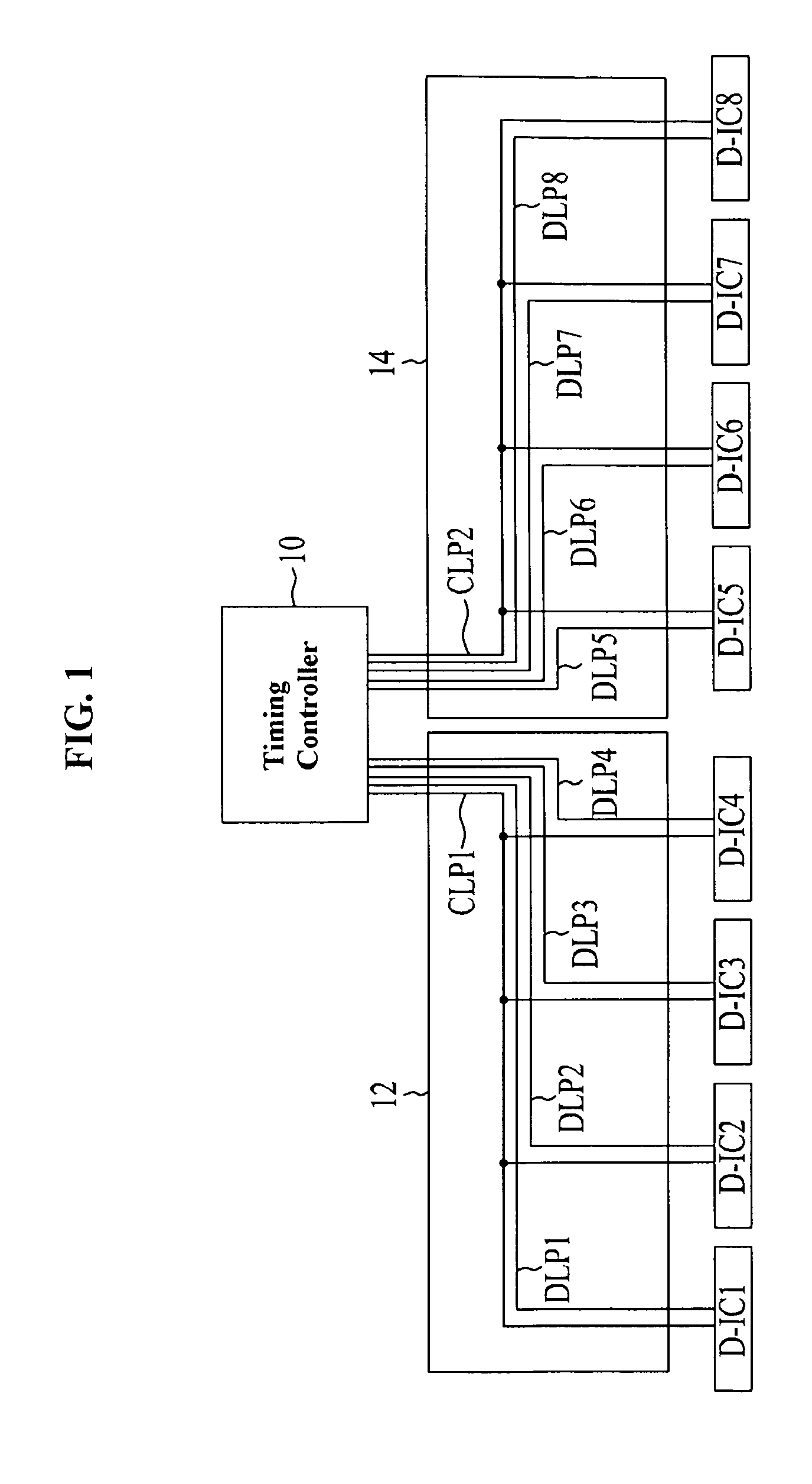
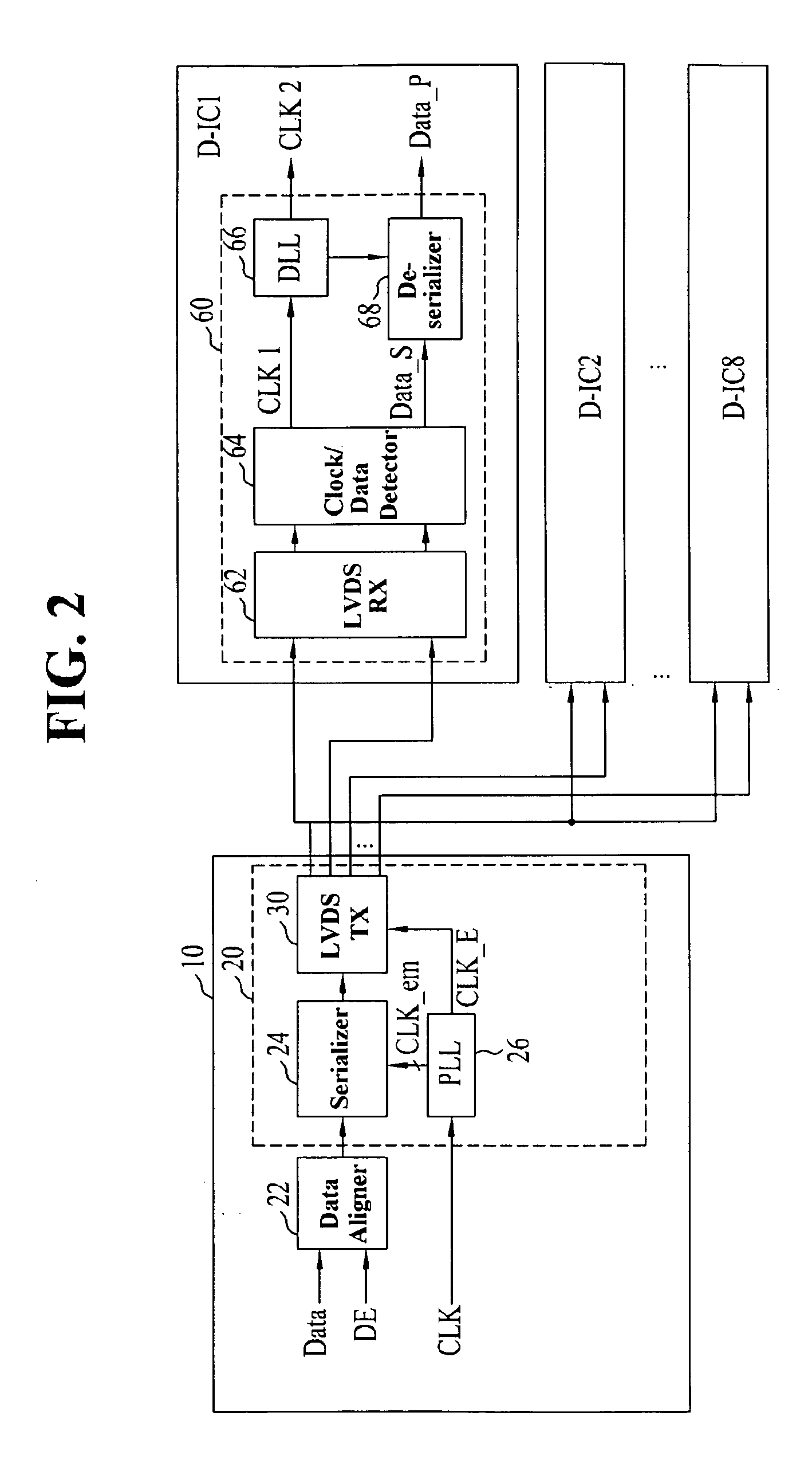
[0050]The data interface apparatus of the flat panel display device shown in FIG. 1 includes a timing controller 10, and a plurality of data integrated circuits (ICs) D-IC1 to D-IC8 for driving data lines of a display panel included in the flat panel display device under the control of the timing controller 10.
[0051]The timing controller 10 is connected to the data ICs D-IC1 to D-IC8 via a plurality of data transfer line pairs DLP1 to DLP8 in a point-to-point manner, respectively. The data ICs D-IC1 to D-IC8 are grouped into two groups, namely, a first group including the data ICs D-IC1 to D-IC4 and a second group including the data ICs D-IC5 to D-IC8. Similarly, the data transfer line pairs DLP1 to DLP8 are grouped into two groups, namely, a first group including the data transfer line pairs DLP1 to DLP4 and a second grou...
second embodiment
[0067]FIG. 4 is a block diagram schematically illustrating an apparatus for data interface of a flat panel display device in accordance with the present invention.
[0068]The data interface apparatus of the flat panel display device shown in FIG. 4 includes a timing controller 110, and a plurality of data ICs D-IC1 to D-IC8 connected to the timing controller 110 via a plurality of data transfer line pairs DLP1 to DLP8 in a point-to-point manner, respectively. Each of the data ICs D-IC1 to D-IC8 independently generates a clock mask signal, to detect a clock embedded in transfer data. In this case, accordingly, the enable transfer line pairs CLP1 and CLP2 used to transfer clock enable signals in the case of FIG. 1 may be dispensed with. Accordingly, it is possible to further reduce the number of transfer lines.
[0069]The data ICs D-IC1 to D-IC8 are grouped into two groups, namely, a first group including the data ICs D-IC1 to D-IC4 and a second group including the data ICs D-IC5 to D-IC8...
PUM
 Abstract
Description
Claims
Application Information