Horizontal Row Drivers For CMOS Image Sensor With Tiling On Three Edges

a technology of cmos image sensor and horizontal row driver, which is applied in the field of large cmos image sensor, can solve the problems of reducing the fill factor of the resulting image sensor, and achieve the effect of improving the fill factor and improving the pixel sensitivity

Active Publication Date: 2009-07-16
TOWER SEMICONDUCTOR
View PDF8 Cites 19 Cited by
  • Summary
  • Abstract
  • Description
  • Claims
  • Application Information

AI Technical Summary

Benefits of technology

[0006]Accordingly, the present invention provides a CMOS image sensor die having a pixel array that extends to three edges of the die. All control circuitry, including row driver circuitry, is located along a fourth edge of the die. None of the control circuitry required to access the pixel array is located within the pixel array, thereby providing an improved fill factor and eliminating the need for pixel interpolation within the pixel array. The present invention thereby provides improved pixel sensitivity without losing image resolution, and enables consistent spacing of pixels throughout the pixel array.

Problems solved by technology

However, Fossum et al. require that the image sensor area of each chip include a centralized row-local control portion, which runs up the center of the image sensor area, such that the central two pixels of each image sensor chip are masked (i.e., missing).
Including this logic in the pixel array undesirably reduces the fill factor of the resulting image sensor.

Method used


Image

  • Horizontal Row Drivers For CMOS Image Sensor With Tiling On Three Edges
  • Horizontal Row Drivers For CMOS Image Sensor With Tiling On Three Edges
  • Horizontal Row Drivers For CMOS Image Sensor With Tiling On Three Edges

Examples


Embodiment Construction

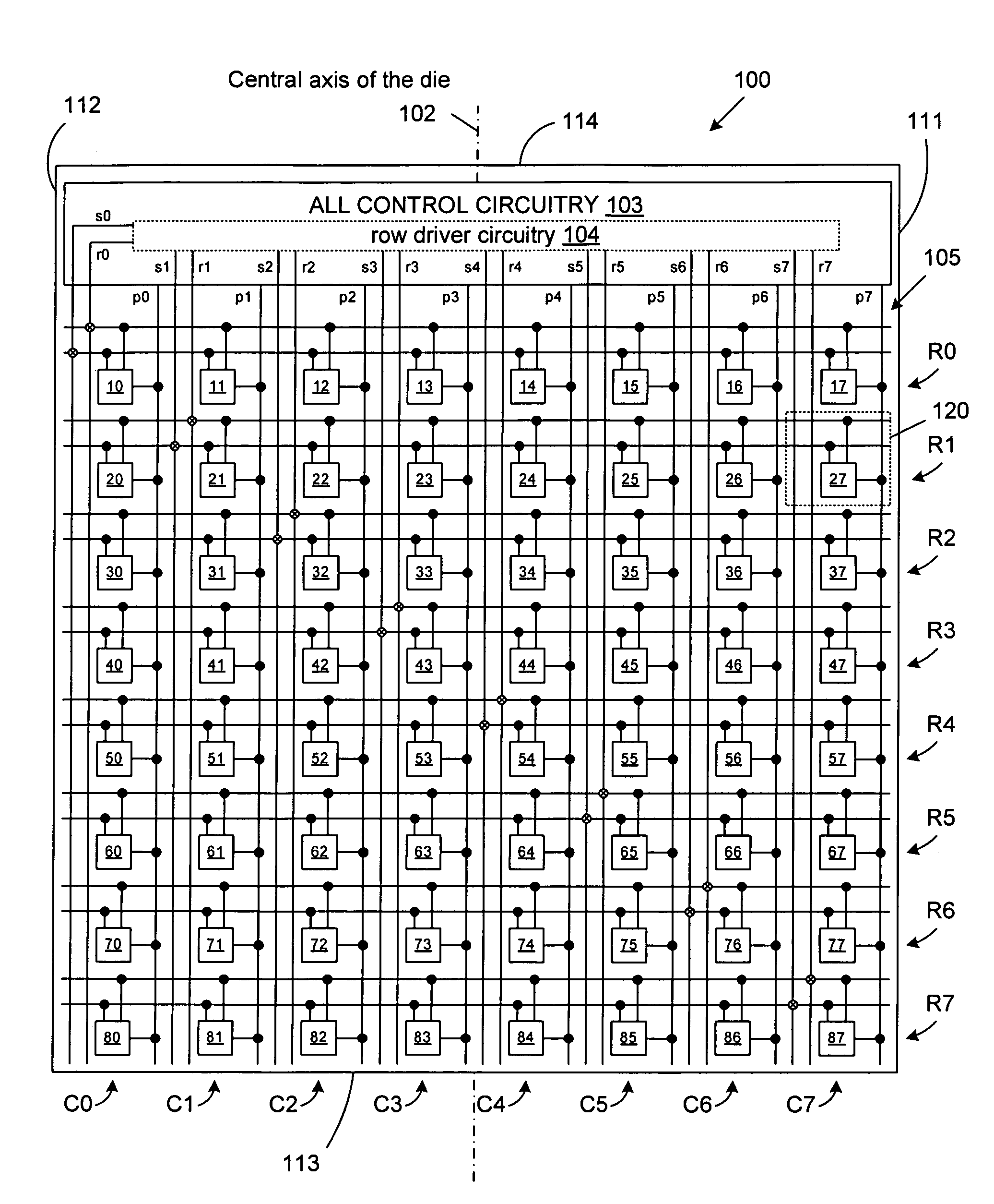
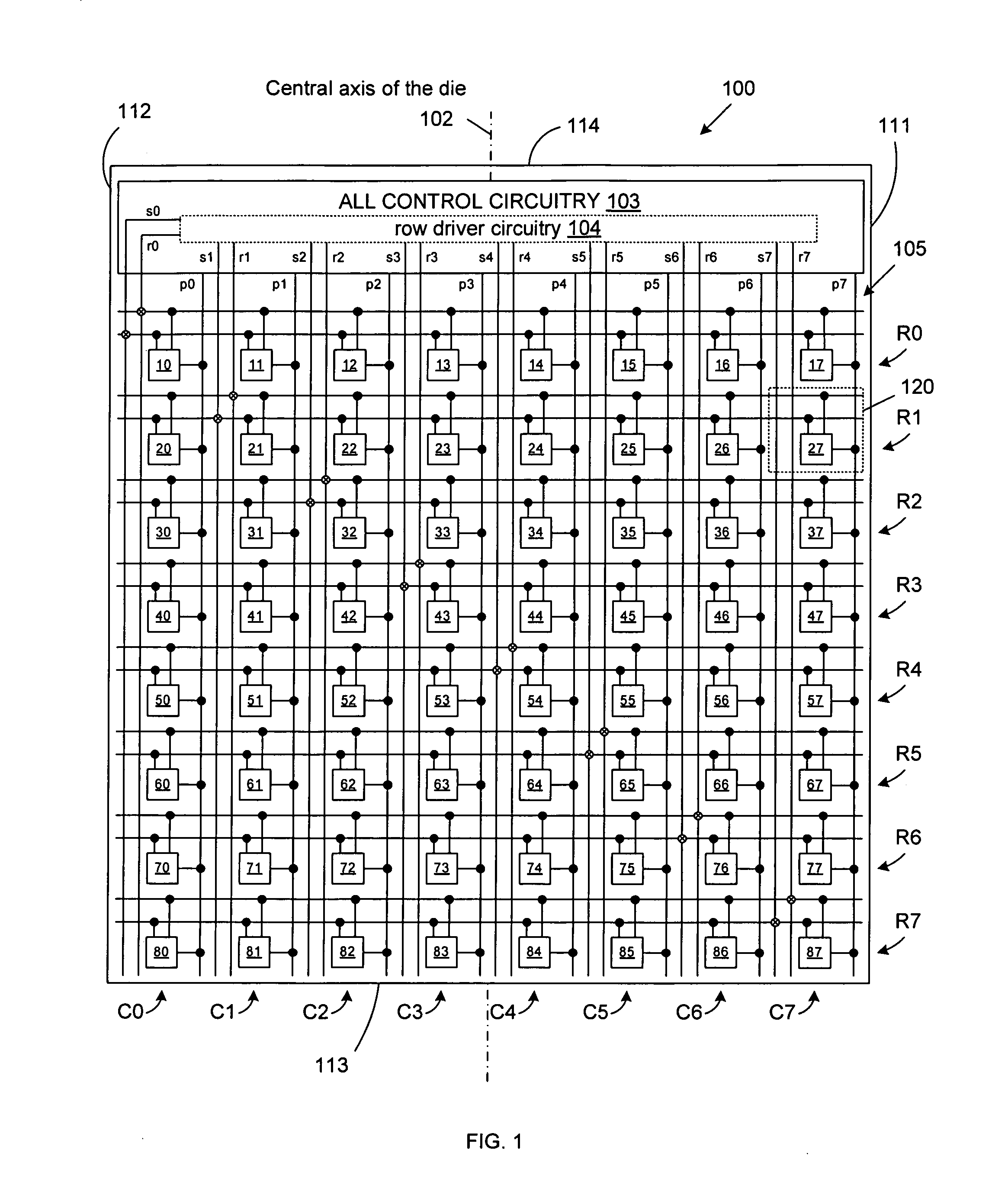
[0014]FIG. 1 is a block diagram of a CMOS image sensor die 100 in accordance with one embodiment of the present invention.

[0015]As used, herein, the term ‘die’ refers to a continuous substrate on which a pixel array and the associated control circuitry is fabricated. A die can have various shapes and sizes, and is not necessarily limited by the exposure area of a reticle used in the corresponding photolithographic process. That is, a die can be made larger than the reticle exposure area of a photolithographic process by implementing a conventional stitching process. This relationship is illustrated in FIG. 2.

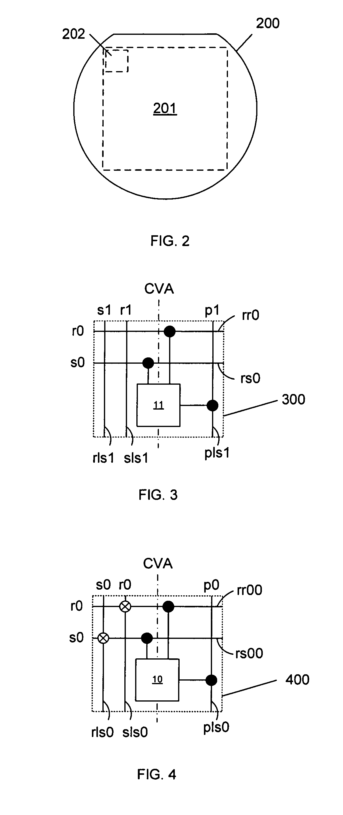
[0016]FIG. 2 is a schematic view of a conventional semiconductor wafer 200, wherein region 202 represents the maximum exposure area of a reticle used in a photolithographic system used to process wafer 200. Typically, one or more entire dies may be fabricated within region 202. However, multiple reticle exposure areas can be ‘stitched’ together to create larger die sizes. For ex...


PUM


Abstract

A large image sensor structure is created by tiling a plurality of image sensor dies, wherein each of the image sensor dies includes a pixel array that extends to three edges of the die, and control circuitry located along a fourth edge of the die. None of the control circuitry required to access the pixel array (e.g., none of the row driver circuitry) is located in the pixel array, thereby enabling consistent spacing of pixels across the pixel array. Because the pixel array of each image sensor die extends to three edges of the die, the pixel array of each image sensor die can abut up to three pixel arrays in other image sensor dies to form a large image sensor structure having 2×N tiled image sensor dies.

Description

FIELD OF THE INVENTION[0001]The present invention relates to large CMOS image sensors that created by tiling a plurality of CMOS image sensor dies.RELATED ART[0002]Some digital imaging applications, such as fluoroscopy or angioscopy, require the use of large digital image sensors. In order to implement large digital image sensors using CMOS imaging technology, multiple CMOS image sensors must be tiled (i.e., mounted adjacent to one another in an array configuration).[0003]U.S. Pat. No. 7,009,646 to Fossum et al. describes a three-sided buttable CMOS image sensor chip, which can be tiled to create a large digital image sensor. However, Fossum et al. require that the image sensor area of each chip include a centralized row-local control portion, which runs up the center of the image sensor area, such that the central two pixels of each image sensor chip are masked (i.e., missing). Fossum et al. further require a two pixel interpolator to interpolate for the missing pixels along the ce...

Claims


Application Information

Patent Timeline
Patent Type & Authority Applications(United States)
IPC IPC(8): H01L27/146H01L31/18
CPCH01L27/14643
Inventor SARIG, EREZRESHEF, RAZALFASSI, SHAYCOHEN, DAVID
Owner TOWER SEMICONDUCTOR
Why Eureka
Try Eureka