Processing method of flat panel display apparatus

Active Publication Date: 2009-07-16
AU OPTRONICS CORP
View PDF2 Cites 9 Cited by
  • Summary
  • Abstract
  • Description
  • Claims
  • Application Information

AI Technical Summary

Benefits of technology

[0103]In the embodiments of the invention, the initial electron emitting state measuring step and the aging processing step are executed or only the aging processing step is executed. That is, in the invention, by executing the aging processing step, the electron emitting characteristics of the high electron emitting row are actively deteriorated more than the electron emitting characteristics of the low electron emitting row (there is a case where such a phenomenon is called “burning”), thereby uniforming the electron emitting characteristics in the electron emitting regions, setting the electron emitting characteristics in the electron emitting regions to desired electron emitting characteristics, or enabling the electron emitting characteristics to approach the desired electron emitting characteristics. In other words, for example, ununiformity of the electron emitting states in the electron emitting regions near the spacer that has been caused after completion of the manufacturing of the flat panel display apparatus is eliminated by using the “burning” which occurs by applying the high voltage to the electron emitting regions for a long time, or by using the “burning” which occurs by applying the high voltage to the electron emitting regions locating at the positions away from the spacer for a long time. Since a ratio of the deterioration is small, it does not exert an adver

Problems solved by technology

Therefore, unless the spacers 40 are disposed between the anode panel AP and the cathode panel CP, the display apparatus will be damaged by the atmospheric pr

Method used


Image

  • Processing method of flat panel display apparatus
  • Processing method of flat panel display apparatus
  • Processing method of flat panel display apparatus

Examples


embodiment 1

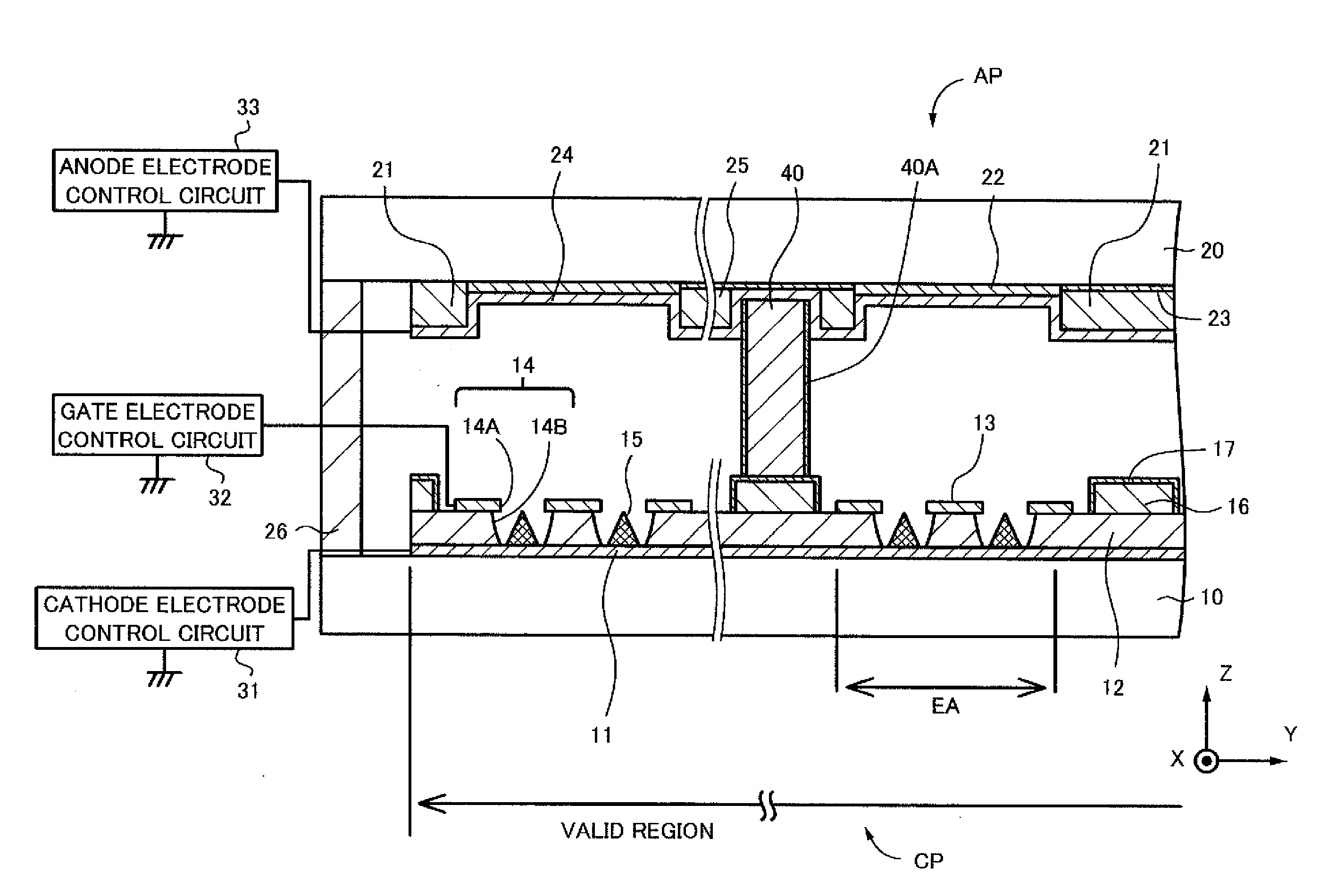
[0139]The embodiment 1 relates to the processing method of the flat panel display apparatus according to each of the first aspect and the second aspect of the invention, and more specifically speaking, it relates to the first construction.

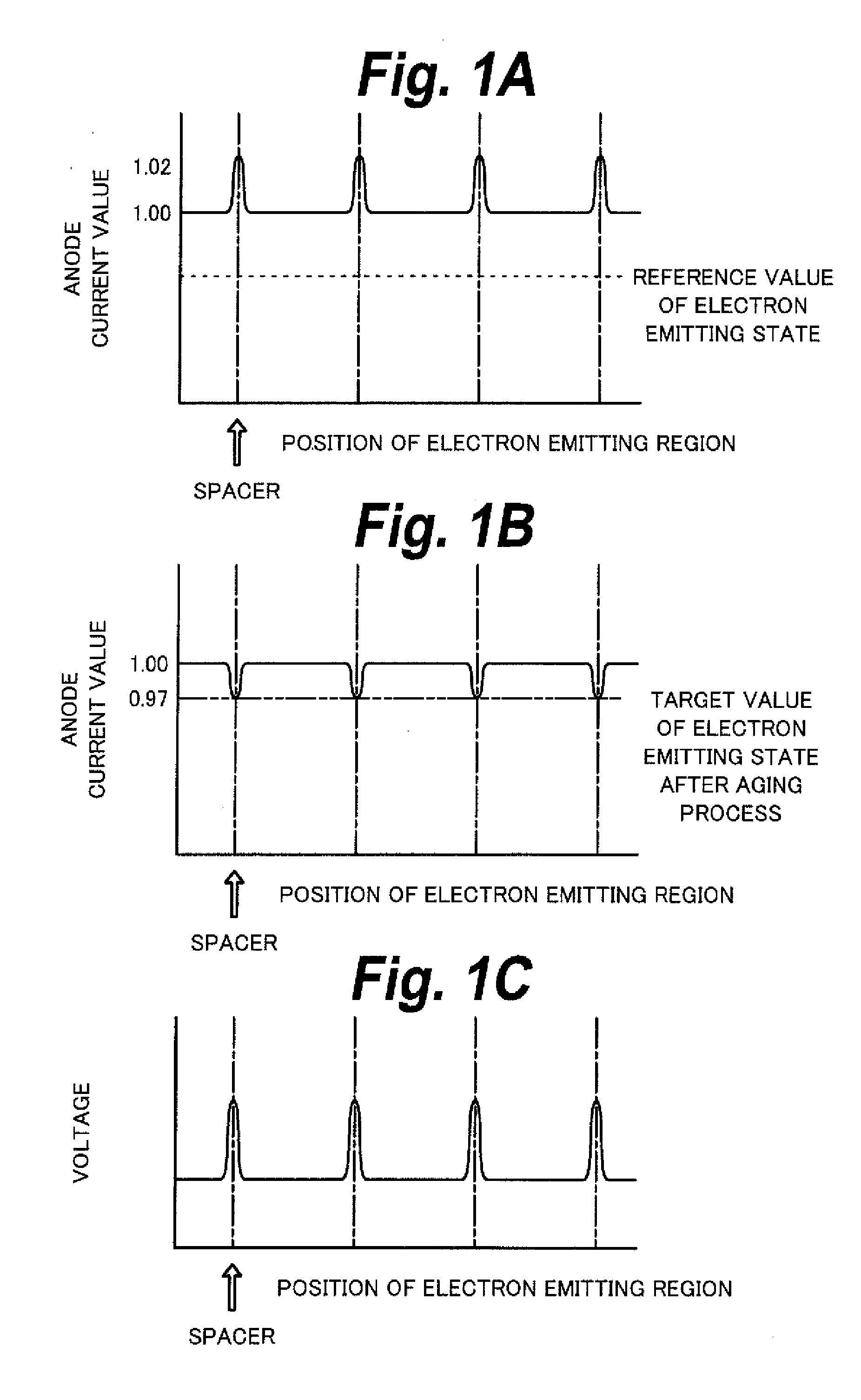
[0140]That is, in the processing method of the flat panel display apparatus according to each of the embodiment 1 or embodiments 2 to 4, which will be explained hereinafter, first, the initial electron emitting state measuring step wherein a predetermined voltage is applied to each electron emitting region EA to thereby allow the electrons to be emitted from each electron emitting region EA, and in a predetermined row, the initial electron emitting states in the electron emitting regions EA are measured is executed.

[0141]In the embodiment 1 or the embodiments 2 to 4, which will be explained hereinafter, the line-sequential driving system is used in the initial electron emitting state measuring step. Specifically speaking, assuming that the number o...

embodiment 2

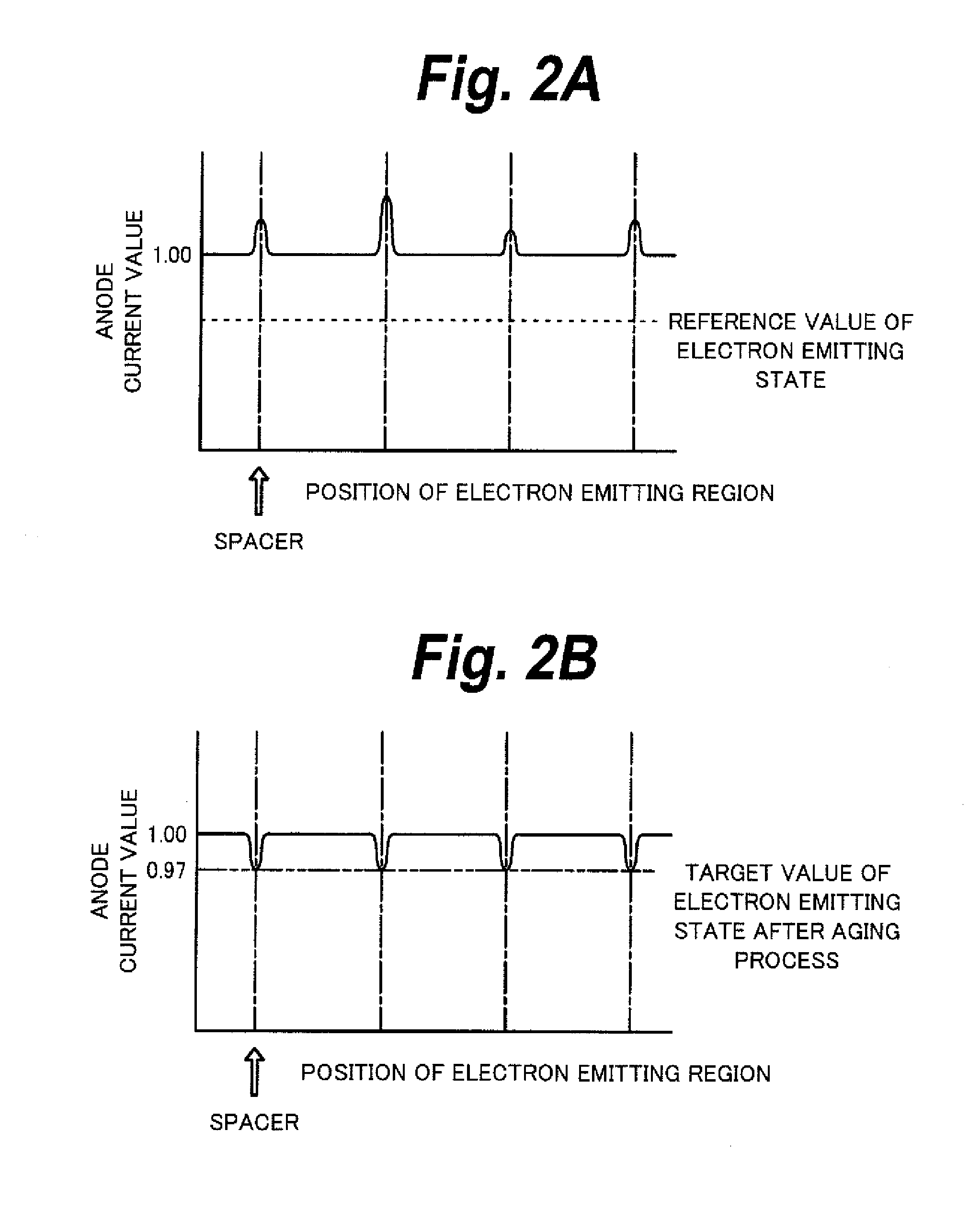
[0156]The embodiment 2 is a modification of the embodiment 1. In the embodiment 1, the case where there is hardly any variation in each of the initial electron emitting states in the high electron emitting row and the initial electron emitting states in the low electron emitting row which were obtained in the initial electron emitting state measuring step has been described. In the embodiment 2, first, the initial electron emitting state measuring step is executed in a manner similar to the embodiment 1. Measurement results of the obtained initial electron emitting states are schematically shown in FIGS. 2A and 3A. There are large variations in the initial electron emitting states in the high electron emitting row. However, also in the embodiment 2, the electron emitting region EA locating near the spacer 40 shows the high initial electron emitting state and the electron emitting region EA locating at the position away from the spacer 40 shows the low initial electron emitting state...

embodiment 3

[0159]The embodiment 3 is also a modification of the embodiment 1 but relates to a second construction. Also in the embodiment 3, there is hardly any variation in each of the initial electron emitting states in the high electron emitting row and the initial electron emitting states in the low electron emitting row which were obtained in the initial electron emitting state measuring step. However, in the embodiment 3, first, the initial electron emitting state measuring step is executed in a manner similar to the embodiment 1. Measurement results of the obtained initial electron emitting states are schematically shown in FIG. 4A. An amount of electrons emitted from the electron emitting region EA locating near the spacer 40 is smaller than an amount of electrons emitted from the electron emitting region EA locating at the position away from the spacer 40. That is, the electron emitting region EA locating near the spacer 40 shows the low initial electron emitting state and the electro...


PUM


Abstract

A processing method of a flat panel display apparatus in which a cathode panel having electron emitting regions and an anode panel having phosphor regions and an anode electrode are joined is provided. A predetermined voltage is applied to each electron emitting region, thereby allowing electrons to be emitted therefrom. In a predetermined row, initial electron emitting states in the electron emitting regions are measured. After that, a voltage higher than that of the electron emitting region in a row showing the low initial electron emitting state is applied to the electron emitting region in the row showing the high initial electron emitting state for a predetermined time, thereby performing aging.

Description

CROSS REFERENCES TO RELATED APPLICATIONS[0001]The present invention contains subject matter related to Japanese Patent Application JP 2008-003227 filed in the Japanese Patent Office on Jan. 10, 2008, the entire contents of which being incorporated herein by reference.BACKGROUND OF THE INVENTION[0002]1. Field of the Invention[0003]The invention relates to a processing method of a flat panel display apparatus.[0004]2. Description of the Related Arts[0005]As an image display apparatus in place of a cathode ray tube (CRT) that is a mainstream at present, various kinds of flat panel display apparatuses are being examined. As such flat panel display apparatuses, for example, a liquid crystal display apparatus (LCD), an electrolumescence display apparatus (ELD), and a plasma display apparatus (PDP) can be mentioned. A flat panel display apparatus in which a cathode panel having electron emitting devices has been assembled is also being developed. As electron emitting devices, a cold cathod...

Claims


Application Information

Patent Timeline
IPC IPC(8): G09G3/30
CPCG09G3/22G09G2320/0233H01J31/127H01J9/42G09G2320/043
Inventor TANAKA, MASANAGA
Owner AU OPTRONICS CORP
Why Eureka
Try Eureka