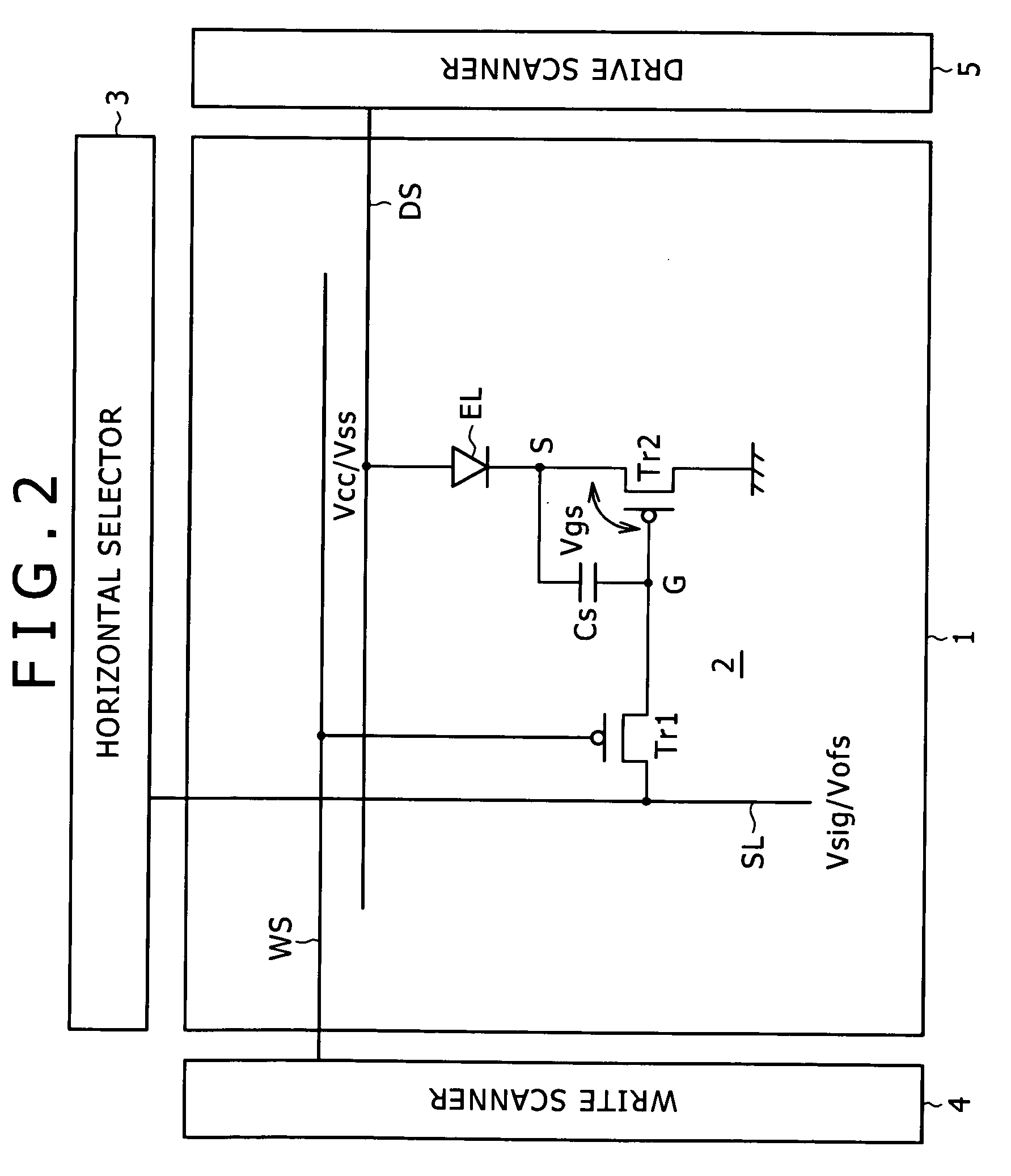
[0009]When the sampling transistor samples the
signal potential from the signal line and holds the potential in the holding
capacitor, the drive current flowing through the drive transistor should preferably be fed back to the holding
capacitor to correct the signal potential so as to correct the drive transistor mobility. The sampling transistor is also a P-channel transistor. The main
scanner removes the
control signal from the
scan line when the signal potential is held in the holding capacitor, bringing the sampling transistor out of conduction and electrically disconnecting the gate of the drive transistor from the signal line. This causes the gate potential of the drive transistor to change with change in the source potential thereof (
bootstrapping action), thus maintaining the gate-to-source potential constant.
[0010]The display device according to the present embodiment has
threshold voltage correction, mobility correction,
bootstrapping and other functions in each of the pixels. The
threshold voltage correction function permits correction of the variation in the threshold
voltage of the drive transistor. Similarly, the mobility correction function permits correction of the variation in the mobility of the drive transistor. Further, the
bootstrapping action of the holding capacitor maintains the
light emission brightness constant at all times during
light emission, irrespective of the changes in the characteristics of the organic EL element. That is, the gate-to-source
voltage of the drive transistor remains constant by the bootstrapping action despite the change in the current-voltage characteristic of the drive transistor over time, thus maintaining the light emission brightness constant.
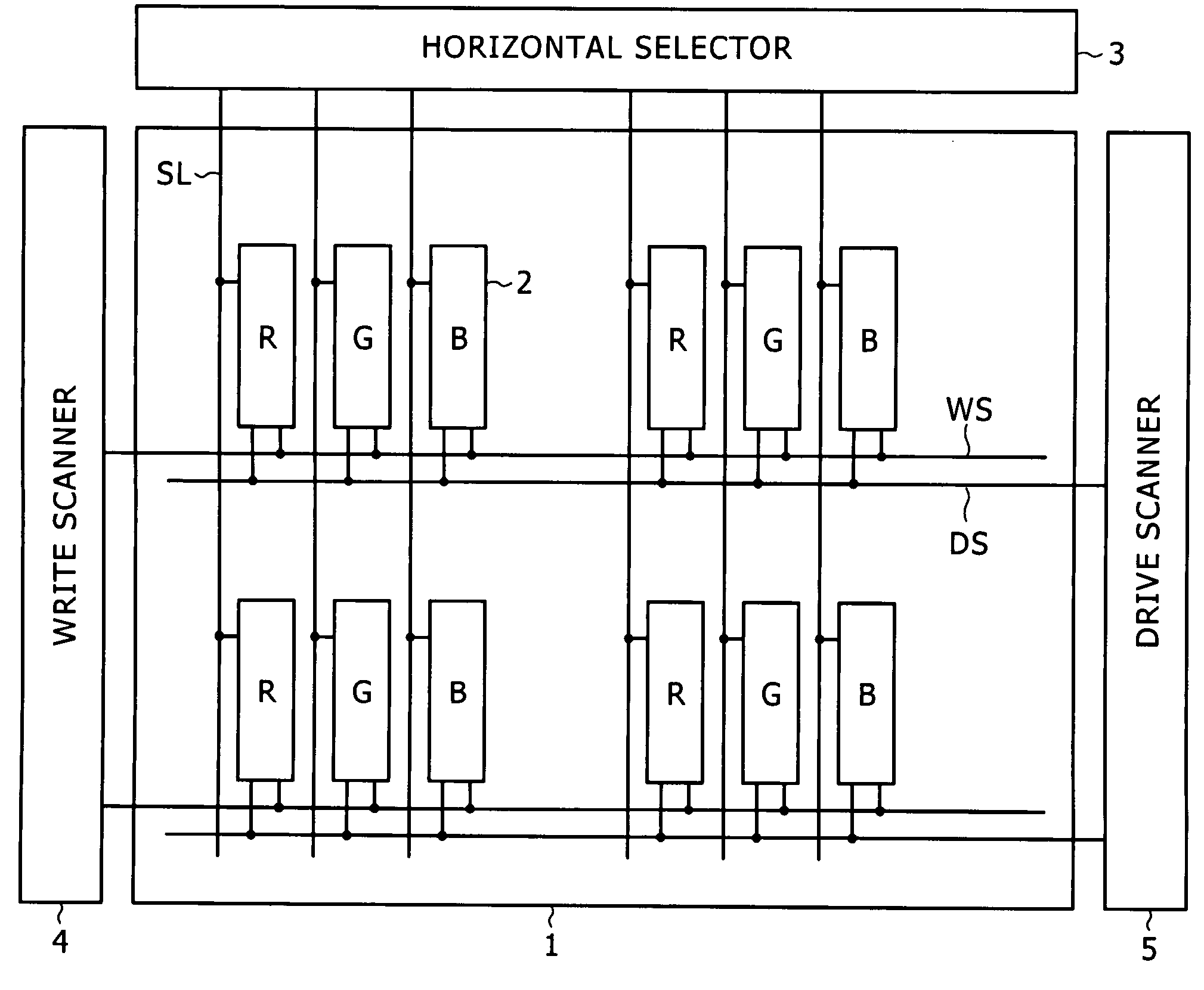
[0011]According to the present embodiment, each of the pixels only includes a light-emitting element, sampling transistor, drive transistor and holding capacitor to provide the threshold voltage correction, mobility correction, bootstrapping and other functions. This has reduced the number of transistor elements to two, which is fewer than in the existing art. The pixel configuration simplified as described above provides the above correction functions. The simplification of the pixel circuit permits reduction of the pixel size, thus allowing to achieve higher definition of the display device.
[0012]In order to simplify the pixel circuit in particular, the drive transistor is a P-channel transistor with the source thereof connected to the
cathode of the light-emitting element. A P-channel transistor has a smaller variation in the threshold voltage and mobility than an N-channel transistor, making it easier to correct the threshold voltage and mobility thereof. Further, the Early effect is less conspicuous in a P-channel transistor than in an N-channel transistor, making the drive current supplied by the drive transistor less susceptible to the
impact of change in supply voltage. As described above, a P-channel transistor for use as the drive transistor minimizes the variation in brightness attributable to a number of factors, thus providing improved screen uniformity.
[0013]To incorporate the threshold voltage correction, mobility correction, bootstrapping and other functions in the present embodiment, the supply voltage supplied to each of the pixels serves as a switching pulse. Using the supply voltage as a switching pulse eliminates the need for a switching transistor adapted to correct the threshold voltage and a
scan line adapted to control the gate of the switching transistor. This ensures significant reduction of pixel circuit components and wirings, thus permitting reduction of the pixel area and achieving higher definition of the display device. Further, the mobility correction is performed simultaneously with the sampling of the video signal potential, thus similarly permitting simplification of the pixel circuit configuration and wirings and contributing to reduced pixel size.

