Manufacture method for semiconductor device with small variation in MOS threshold voltage

a manufacturing method and threshold voltage technology, applied in semiconductor devices, semiconductor/solid-state device details, electrical devices, etc., can solve the problems of affecting the operation of high-speed operation and large operation margin, and unable to reduce the interface state density. , to achieve the effect of facilitating the reduction of the threshold voltage variation

Inactive Publication Date: 2005-05-03
YAMAHA CORP
View PDF19 Cites 7 Cited by
  • Summary
  • Abstract
  • Description
  • Claims
  • Application Information

AI Technical Summary

Benefits of technology

[0016]It is an object of the present invention to provide a novel method of manufacturing a semiconductor device capable of easily lowering a variation in threshold voltages of MOS type transistors.
[0018]During the heat treatment, hydrogen in the hydrogen containing film of the interlayer insulating film is released and diffuses in to the channel region of the MOS transistor to thereby lower interface state density of the channel region. The interlayer insulating film including the hydrogen containing film covers not only the gate electrode layer but also the MOS type transistor and a silicon nitride film to be used as the hydrogen transmission preventing film prevents hydrogen in the hydrogen containing film from diffusing into the upper layer. It is therefore possible to sufficiently lower the interfacial energy levels of the channel region. Further, since the silicon nitride film does not transmit external hydrogen therethrough, it is possible to used a nitrogen gas atmosphere not containing hydrogen, as the heat treatment atmosphere. It is therefore possible to easily lower a variation in threshold voltages of MOS type transistors.
[0020]In the step of forming the wiring layer, a plurality of adjacent wiring layers may be formed, and in the step of forming the silicon nitride film, it may be formed as thin as can cover the wiring layers and form grooves between adjacent wiring layers. Since air having a dielectric constant of 1 is filled in the grooves, a electrostatic capacitance between wiring layers can be reduced. Furthermore, the heat treatment for lowering interfacial energy levels is performed after the silicon nitride film covering the wiring layers is formed. Therefore, even if the wiring layers are made of Al or Al alloy, hillocks are not formed and a short circuit between wiring layers can be avoided.
[0021]The step of forming the interlayer insulating film may form a silicon oxide film made of hydrogen silsesquioxane resin in a ceramic state, as the hydrogen containing film. It is therefore possible to control the hydrogen content in the silicon oxide film as the hydrogen containing film in accordance with the conditions of the heat treatment for changing to the ceramic state. The manufacture yield can thus be improved.
[0022]Hydrogen release characteristics between a heat treatment temperature and a hydrogen release amount of the hydrogen containing film may be prepared in advance to perform the heat treatment at a temperature determined from the hydrogen release characteristics. It is therefore possible to reliably lower the interfacial energy levels and improve the manufacture yield.
[0024]As above, after the wiring layer is formed on the interlayer insulating film including the hydrogen containing film and the surface protection film is formed on the interlayer insulating film, covering the wiring layer, heat treatment for lowering interfacial energy levels is performed. Accordingly, it is not necessary for the heat treatment atmosphere to contain hydrogen, and a variation in threshold voltages of MOS type transistors can be lowered.

Problems solved by technology

A channel region of a MOS transistor may have process damages during manufacture.
Therefore, the electrostatic capacitance between the wiring layers 2A and 2B becomes large, which hinders a high speed operation and a large operation margin.
However, if the silicon nitride film 3 is made thin, the hydrogen annealing process for lowering interfacial energy levels is associated with the following problems.
On the other hand, if the hydrogen annealing process is performed after the silicon nitride film 3 is formed, interface state density cannot be lowered because hydrogen is hard to transmit through the silicon nitride film 3.
Although this unreacted hydrogen released by the hydrogen annealing process contributes to lowering the interfacial energy levels, the contribution degree is insufficient.
It is necessary to provide two hydrogen supply sources and the process control becomes complicated.
Therefore, this film cannot be utilized as the hydrogen supply source during the hydrogen annealing process.
In other words, the salicide process cannot be adopted if the film C is used as the hydrogen supply source.

Method used


Image

  • Manufacture method for semiconductor device with small variation in MOS threshold voltage
  • Manufacture method for semiconductor device with small variation in MOS threshold voltage
  • Manufacture method for semiconductor device with small variation in MOS threshold voltage

Examples


Embodiment Construction

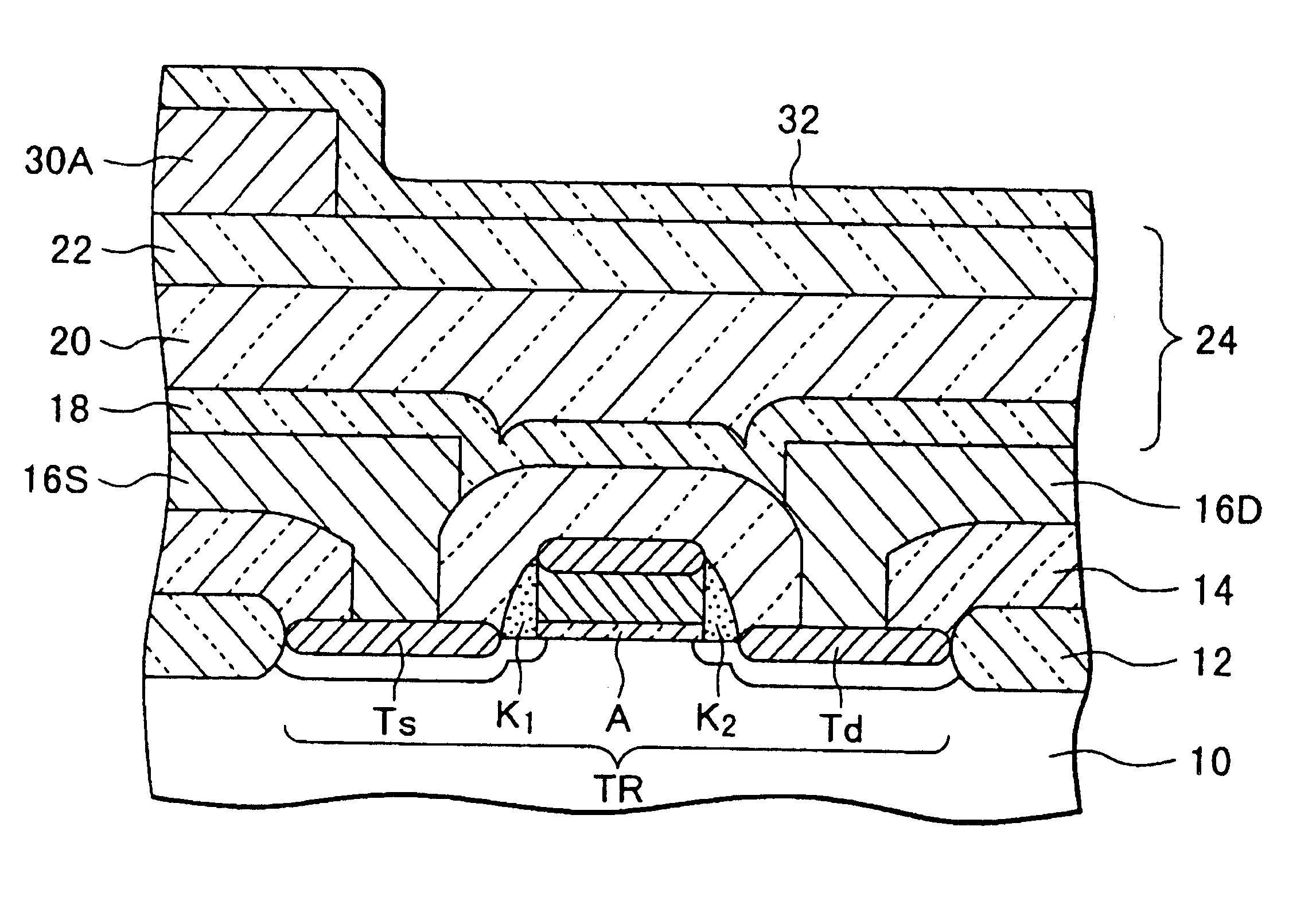
[0041]A MOS type IC manufacture method according to an embodiment of the invention will be described with reference to FIG. 1, FIGS. 2A to 2I and FIG. 3.

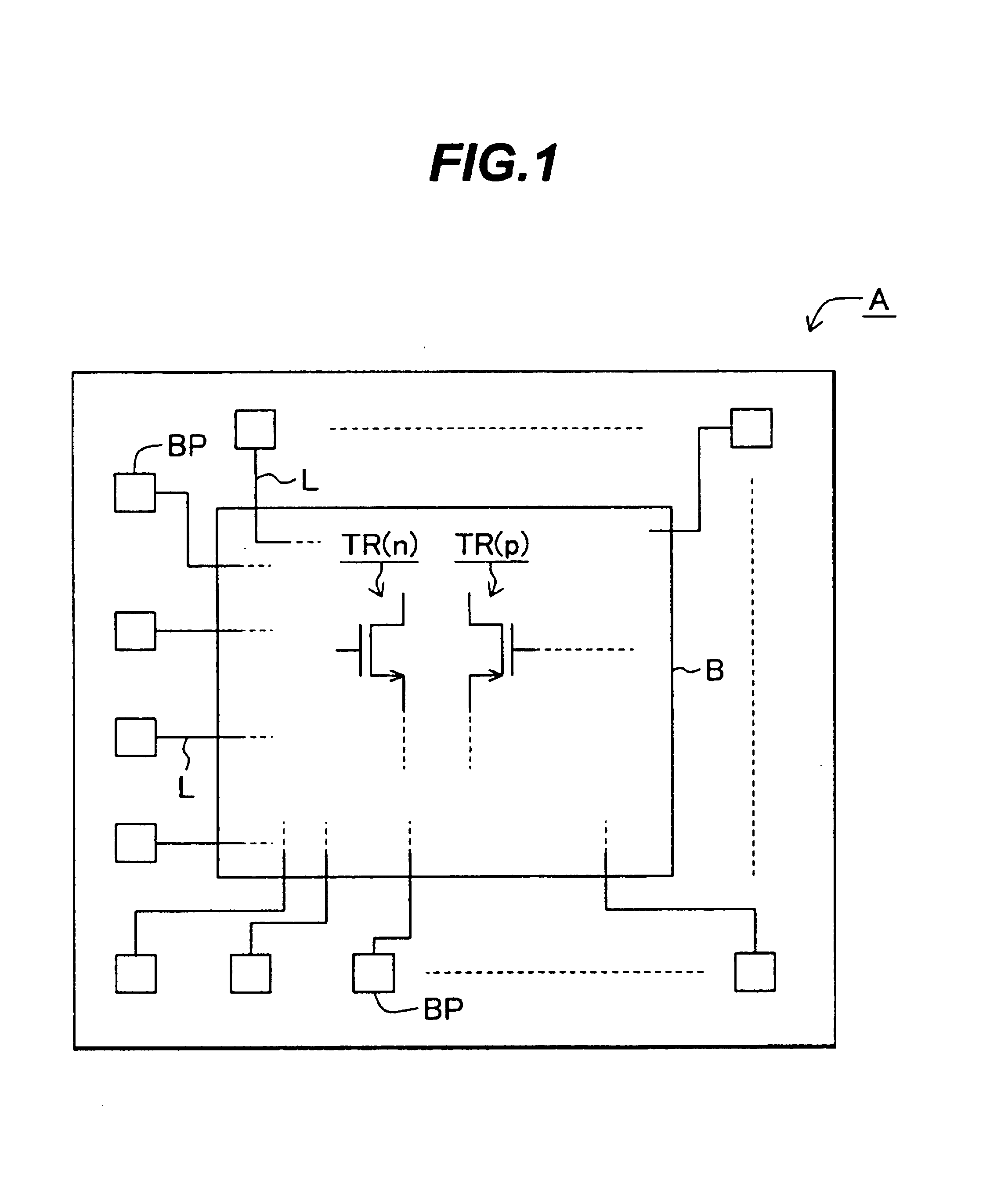
[0042]FIG. 1 is a schematic plan view of a MOS type IC. As shown in FIG. 1, a MOS type IC A has an integrated circuit area B formed with an integrated circuit, and a number of bonding pads BP disposed around the integrated circuit area B. The integrated circuit in the integrated circuit area B has a number of MOS transistors. A CMOS type IC is made of basic CMOS circuits each constituted of pairs of one n-channel MOS transistor TR(n) and one p-channel MOS transistor TR(p). Transistors, CMOS circuits and bonding pads BP are electrically connected by wiring patterns L.

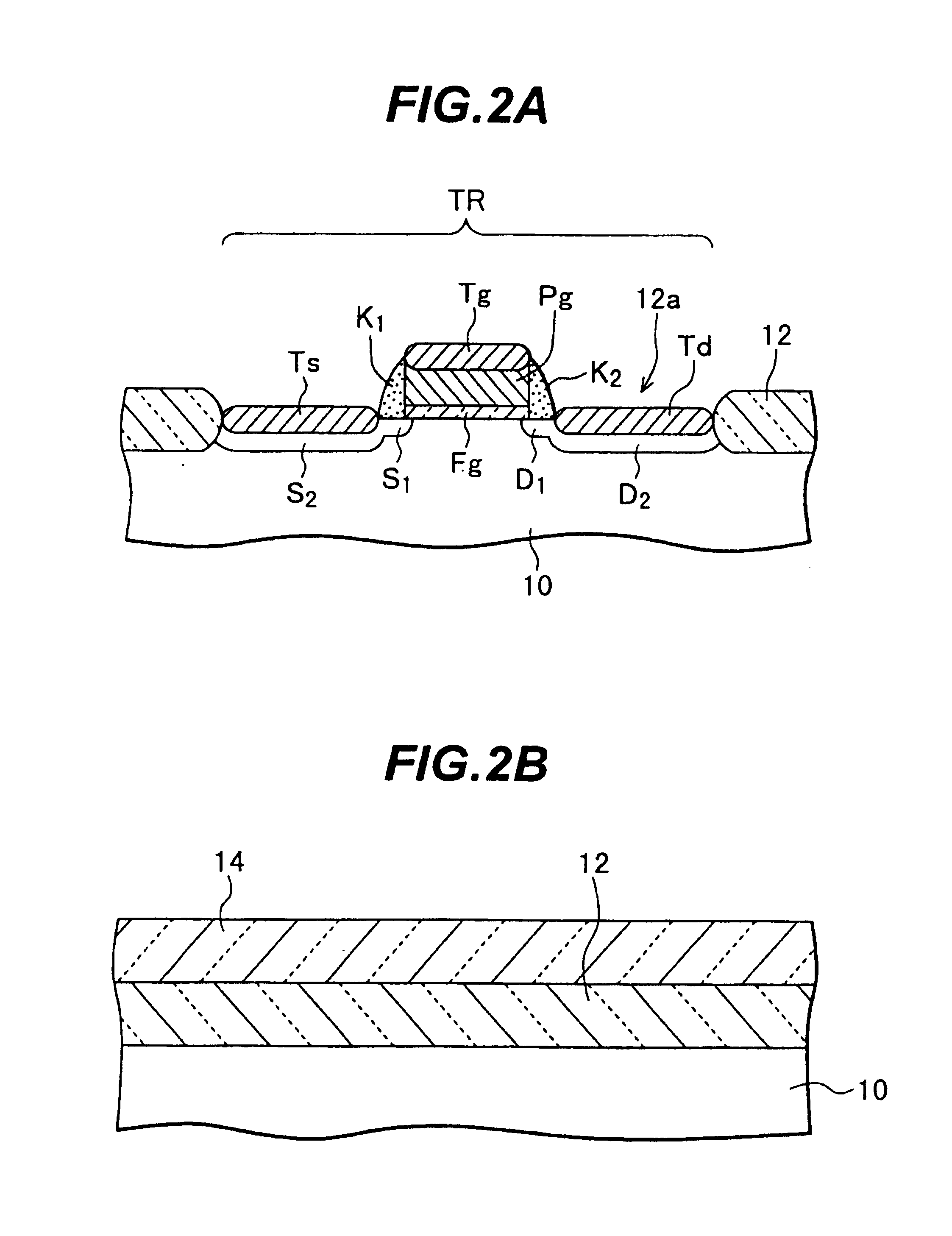
[0043]Next, a manufacture method for a CMOS circuit will be described. As shown in FIG. 2A, on the surface of a semiconductor substrate 10 made of, for example, silicon, a field insulating film (silicon oxide film) 12 defining an active region 12a is formed by LOCOS. For...


PUM


Abstract

After a MOS type transistor is formed on the surface of a semiconductor substrate, an interlayer insulating film covering the transistor is formed. The insulating film includes a silicon oxide film made of hydrogen silsesquioxane resin in a ceramic state. After a wiring layer is formed on the insulating film, a silicon oxide film as a surface protection film is formed on the insulating film, covering the wiring layer. In order to reduce process damages, heat treatment is performed 30 minutes at 400° C. in a nitrogen gas atmosphere. With this heat treatment, hydrogen in the silicon oxide film is released and diffuses into the channel region of the transistor to lower interfacial energy levels. Since the silicon nitride film does not transmit hydrogen, it is not necessary for the heat treatment atmosphere to contain hydrogen. A variation in threshold voltages of MOS type transistors can be easily lowered.

Description

[0001]This application is based on Japanese Patent Application HEI 11-055341 filed on Mar. 3, 1999, all the contents of which are incorporated herein by reference.BACKGROUND OF THE INVENTION[0002]a) Field of the Invention[0003]The present invention relates to a method of manufacturing a semiconductor device with MOS transistors (insulated gate type field effect transistors), and more particularly to techniques capable of easily lowering a variation in threshold voltages of MOS transistors by forming a wiring layer on an interlayer insulating film including a hydrogen containing film, forming a silicon nitride film as a surface protection film (passivation film) on the wiring layer, and thereafter performing heat treatment to lower interface state density.[0004]b) Description of the Related Art[0005]In a semiconductor device having a surface protection film, for example, as shown in FIG. 6, on the surface of an interlayer insulating film 1, wiring layers 2A and 2B near to each other ...

Claims


Application Information

Patent Timeline
Patent Type & Authority Patents(United States)
IPC IPC(8): H01L21/02H01L21/30H01L23/28H01L23/31H01L21/70H01L21/28H01L21/768H01L21/316H01L23/00H01L23/52H01L21/318H01L23/532H01L21/314H01L21/312H01L23/522H01L21/336H01L29/78
CPCH01L21/28176H01L21/3003H01L21/316H01L21/76801H01L21/76828H01L21/76829H01L21/76834H01L23/3171H01L23/564H01L2924/0002H01L21/3124H01L21/3185H01L23/53223H01L23/5329H01L2924/00H01L21/02129H01L21/02134H01L21/02164H01L21/0217H01L21/022H01L21/02271H01L21/02274H01L21/02282H01L21/02337H01L21/02216
Inventor YAMAHA, TAKAHISA
Owner YAMAHA CORP
Why Eureka
Try Eureka