Semiconductor memory device

a memory device and semiconductor technology, applied in semiconductor devices, digital storage, instruments, etc., can solve the problems of limiting the number of writing operations, high power consumption needed for retaining data during a standby period, and cannot be used in a case where the writing operation is not used, so as to reduce the voltage gap and reduce the power consumption for holding data.

Inactive Publication Date: 2015-10-13
SHARP KK
View PDF4 Cites 5 Cited by
  • Summary
  • Abstract
  • Description
  • Claims
  • Application Information

AI Technical Summary

Benefits of technology

[0024]According to the semiconductor memory device having the above characteristics, the memory voltage having the constant relationship with the writing voltage inputted to the data signal line is stored in the memory node. More specifically, the switching element is turned on, and the second transistor element of the memory cell in the selected row is turned on to selectively initialize the memory node of that memory cell at the predetermined initialization voltage, and then the switching element is turned off, so that the drain electrode and the gate electrode of the first transistor element are connected through the second transistor element, and the first transistor element serves as a diode. In a case where a conductivity type of the first transistor element is an n type, the diode is provided such that an anode is connected to the memory node, and a cathode is connected to the data signal line, while in a case where the conductivity type of the first transistor element is a p type, the diode is provided such that an anode is connected to the data signal line, and a cathode is connected to the memory node. In either case, a turn-on voltage of the diode is equal to an absolute value of a threshold voltage of the first transistor element. Therefore, the initialization voltage is previously set such that the voltage difference between the initialization voltage and the writing voltage of the memory node is larger than the turn-on voltage of the diode regardless of the writing voltage. In this case, when the data signal line is driven at the writing voltage in the writing operation, and the diode is turned on, the voltage of the memory node of the memory cell in the selected row is reduced from the initialization voltage to the writing voltage until the diode is turned off in the case where the conductivity type of the first transistor element is the n type, while the voltage of the memory node of the memory cell in the selected row is increased from the initialization voltage to the writing voltage until the diode is turned off in the case where the conductivity type is the p type. As a result, in the writing operation, the memory voltage having the specific relationship with the writing voltage is stored in the memory node, and more specifically, in the case where the conductivity type of the first transistor element is the n type, the memory voltage is higher and in the case where the conductivity type of the first transistor element is the p type, the memory voltage is lower than the writing voltage by the threshold voltage of the first transistor element. Therefore, in the initialization operation and the writing operation, the memory voltage having the specific relationship with the writing voltage is stored in the memory node only by switching the on / off of the switching element.
[0025]After the memory voltage is stored in the memory node, the memory node is set to a floating state by turning off the second transistor element, so that the charge corresponding to the memory voltage can be continuously held. Here, since the second transistor element is the oxide semiconductor transistor whose leak current is extremely small compared to the silicon transistor, so that the charge corresponding to the memory voltage stored in the memory node can be held stably for a long time, and power consumption for holding the data can be considerably reduced, and as a result, it can be functioned as a nonvolatile memory.
[0026]Furthermore, in the reading operation, under the condition that the second transistor element is turned off and the memory node is maintained in the floating state, the switching element connected to the memory cell selected as a reading target through the first control line is turned on, and the second selection voltage is applied to the second selection line connected to the memory cell in the selected row selected as the reading target so that a voltage state of the memory node of the selected memory cell is returned to the state provided right after the memory voltage has been written in the writing operation. Thus, when a current is applied to the data signal line through the switching element and the first transistor element, the reading voltage or the reading current stored in the memory node and corresponding to the memory voltage can be outputted to the data signal line.
[0027]In the reading operation to output the reading voltage to the data signal line, the data signal line is previously set to the floating state so that its voltage level can be changed when the voltage is charged or discharged with the reading current flowing between the drain electrode and the source electrode of the first transistor element. Thus, when the voltage of the data signal line is charged or discharged to the same voltage level as the writing voltage in the writing operation, the voltage difference between the gate electrode (memory node) and the source electrode (data signal line) of the first transistor element becomes equal to an absolute value of the threshold voltage of the first transistor element, so that the first transistor element is cut off, and the charge or discharge is finished, and as a result, the reading voltage having the same voltage as the writing voltage is outputted to the data signal line.
[0028]Meanwhile, in the reading operation to output the reading current to the data signal line, when a bias condition of the first control line is adjusted so that the first transistor element may reach a saturation state in the reading operation, the reading current flowing between the drain electrode and the source electrode of the first transistor element can be a saturation current which is proportional to a square of the voltage difference between the voltage between the gate electrode and the source electrode, and the threshold voltage of the first transistor element. Here, the memory voltage stored in the memory node differs from the writing voltage applied in the writing operation by the absolute value of the threshold voltage of the first transistor element, so that the reading current is proportional to a square of a voltage difference between the writing voltage and the voltage applied to the data signal line in the reading operation. Thus, the reading current corresponding to the writing voltage, that is, corresponding to the information stored in the memory node can be outputted.
[0029]Here, it is to be noted that since the memory voltage stored in the memory node is higher or lower by the threshold voltage of the first transistor element in each memory cell, the variation in the threshold voltage of the first transistor element has been previously compensated, so that the reading voltage and the reading current outputted to the data signal line in the reading operation do not contain a voltage component and a current component which depend on the threshold voltage of the first transistor element, and they are not affected by the threshold voltage of the first transistor element. As a result, according to the semiconductor memory device having the above characteristics, it is possible to reduce a voltage gap among the writing voltages corresponding to the respective values of the multilevel information, so that the operation can be performed at lower voltage or when the operation is performed at the same voltage, the information can be further multilevel information.

Problems solved by technology

As for the RAM, there is no limit on the number of writing operations, but it has the problem that retained data is lost at the time of power-supply disconnection, so that high power consumption is needed for retaining data during a standby period.
Meanwhile, as for the ROM, data can be retained at the time of power-supply disconnection, but there is a limit on the number of writing operations, so that it cannot be used for a case where the writing operations are frequently needed.
Therefore, research and development have been carried out for an ideal NVRAM (Nonvolatile Random Access Memory) through the ages because there is no limit on the number of writing operations and written data can be retained with super-low power consumption, but it has not been commercialized yet.

Method used


Image

  • Semiconductor memory device
  • Semiconductor memory device
  • Semiconductor memory device

Examples


first embodiment

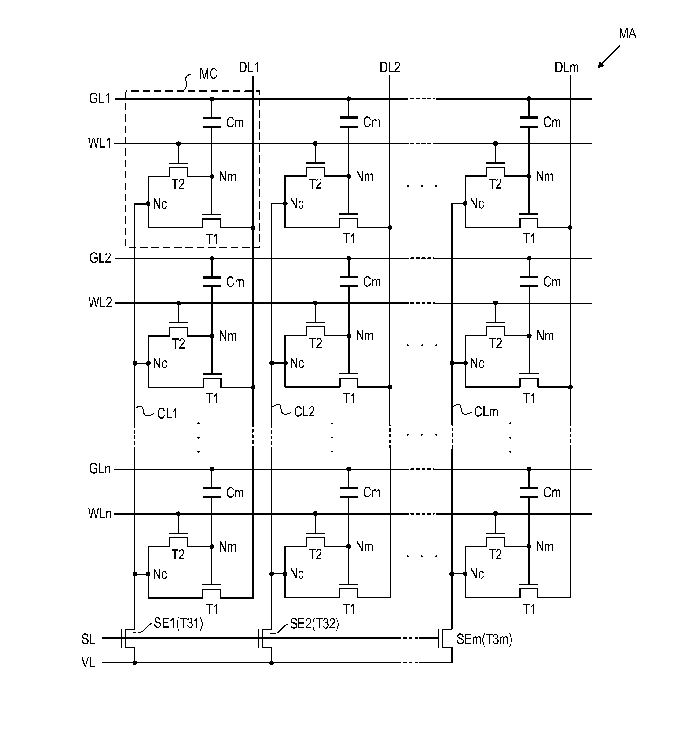
[0047]In the first embodiment, a description will be given to a semiconductor memory device in the present invention (hereinafter, simply referred to as the memory device), and a circuit configuration of a memory cell used in the memory device.

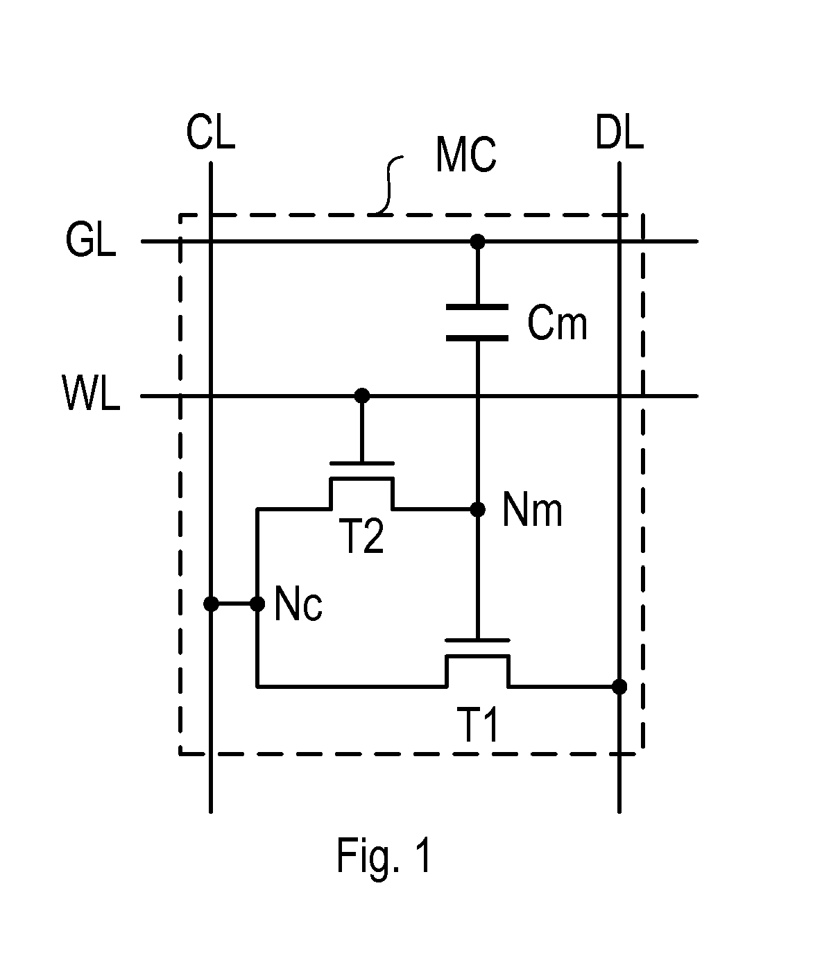
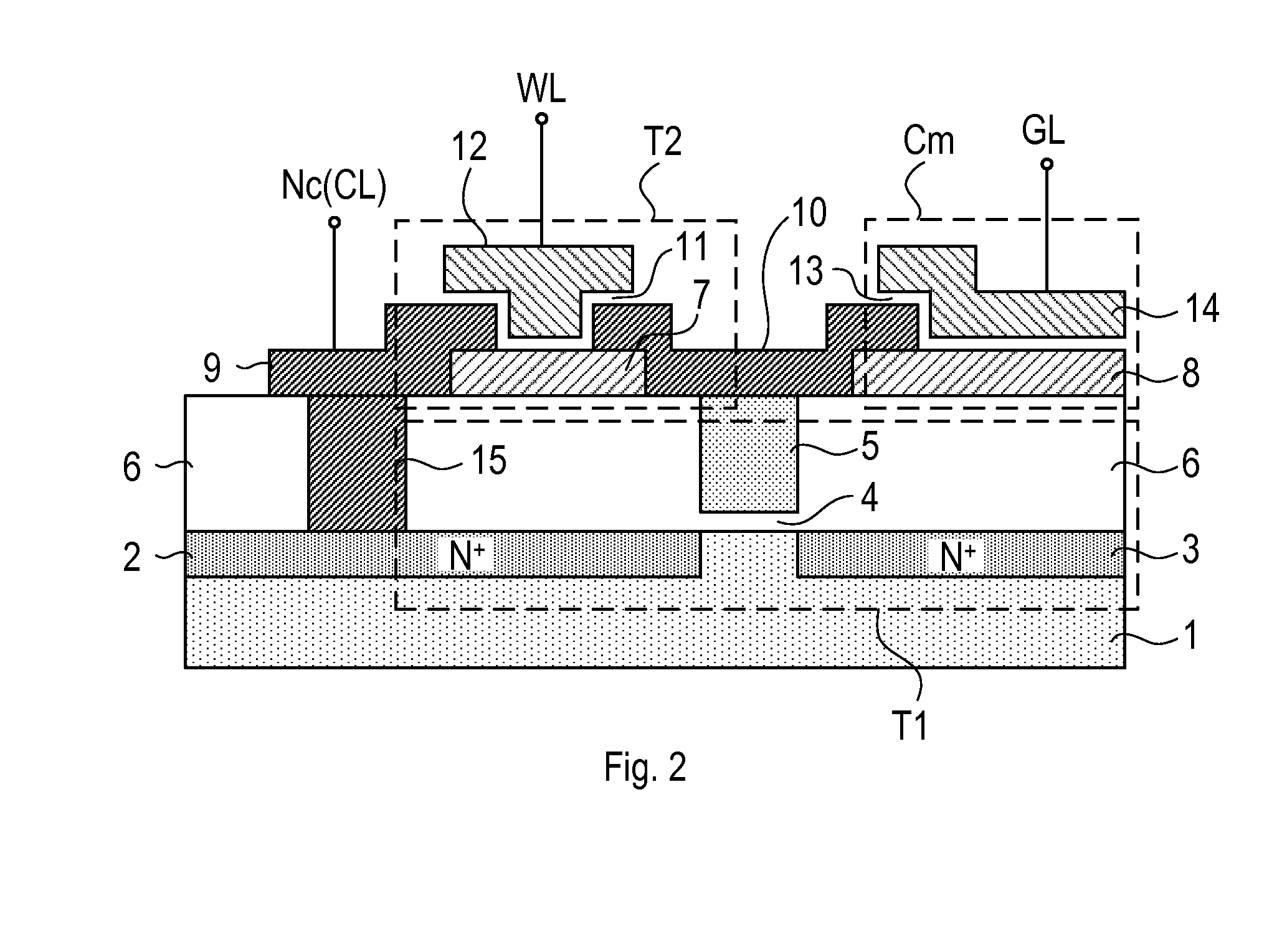
[0048]FIG. 1 shows an equivalent circuit diagram of a memory cell MC. The memory cell MC is provided with a first transistor element T1 composed of an insulated gate FET, a second transistor element T2 composed of an oxide semiconductor insulated gate FET, and a capacitive element Cm. In this embodiment, it is assumed that the first transistor element T1 is an n-channel MOSFET formed on a silicon substrate, and the second transistor element T2 is an n-channel thin film transistor (TFT).

[0049]In addition, as shown in FIG. 1, in the memory cell MC, a memory node Nm is formed at a connection point of a gate electrode of the first transistor element T1, a source electrode of the second transistor element T2, and one end of the capacitive element C...

second embodiment

[0071]In the second embodiment, a detailed description will be given to the initialization operation, the writing operation, and the reading operation, for the memory cell array MA, in accordance with the circuit configuration of the memory cell MC, the memory cell array MA, and the memory device 20 described in the first embodiment. In the following description, it is assumed that a plurality of bits of the input data inputted as the data input signal DIN are divided to every two bits, and one of four-value data (0 to 3) each having the two bits is written in the one memory cell MC, and one of the four-value data written in each memory cell MC is read. In addition, according to this embodiment, the voltage state of the memory node Nm which has been initialized in the initialization operation is allocated to the one data value “3” in the four-value data, but the initialized voltage state is not necessarily allocated to the one data value.

[0072]In addition, in the following descripti...

third embodiment

[0121]The description has been given to the reading operation in the case where the reading circuit 26 is the voltage detection type sense amplifier in the second embodiment, but in the third embodiment, a description will be given to the reading operation in the case where the reading circuit 26 is the current detection type sense amplifier, with reference to FIGS. 9A to 9C and 10. The initialization operation and the writing operation are the same as descried in the second embodiment. FIG. 10 shows a timing chart in a case where the reading operation is performed for the one selected row after the writing operation has been performed, by selecting one or more data lines DL in the same manner as in FIG. 8. FIGS. 9A to 9C are also applied to the case where the reading circuit 26 is the current detection type sense amplifier.

[0122]In the case where the reading circuit 26 is the current detection type sense amplifier, a voltage condition applied to each signal line is the same as that...


PUM


Abstract

Provided is a semiconductor memory device including an oxide semiconductor insulated gate FET and having a capability to implement advanced performance without being affected by a variation in threshold voltage. A memory cell MC includes a memory node Nm formed at a connection point of a gate of a first transistor element T1, a source of a second transistor element T2, and one end of a capacitive element Cm, and a control node Nc formed at a connection point of a drain of the first transistor element T1 and a drain of the second transistor element T2. Each memory cell MC arranged in the same column includes the control node Nc connected to a shared first control line CL extending in a column direction, the first transistor element T1 having a source connected to a shared data signal line DL extending in the column direction, the second transistor element T2 having a gate connected to an individual first selection line WL, and the capacitive element Cm having the other end connected to an individual second selection line GL, and a switching element SE having one end connected to the first control line CL, and the other end connected to a voltage supply line VL is provided with respect to each first control line CL.

Description

CROSS-REFERENCE TO RELATED APPLICATIONS[0001]This application is a National Phase filing under 35 U.S.C. §371 of International Application No. PCT / JP2013 / 053479 filed on Feb. 14, 2013, and which claims priority to Japanese Patent Application No. 2012-090906 filed on Apr. 12, 2012.TECHNICAL FIELD[0002]The present invention relates to a semiconductor memory device including an oxide semiconductor insulated gate FET (Field Effect Transistor), and more particularly, to a semiconductor memory device suitable for storing multilevel information.BACKGROUND ART[0003]The semiconductor memory device is broadly divided into a RAM (Random Access Memory) and a ROM (Read Only Memory). As for the RAM, there is no limit on the number of writing operations, but it has the problem that retained data is lost at the time of power-supply disconnection, so that high power consumption is needed for retaining data during a standby period. Meanwhile, as for the ROM, data can be retained at the time of power-...

Claims


Application Information

Patent Timeline
Patent Type & Authority Patents(United States)
IPC IPC(8): G11C11/24H01L27/115G11C11/403G11C11/4074G11C16/10H01L29/786H01L27/12G11C16/04
CPCH01L27/11526G11C11/403G11C11/4074G11C16/0408H01L27/115H01L29/7869G11C16/10H01L27/1225G11C16/0433H01L27/1156H10B41/70H10B69/00H10B41/40
Inventor YAMAUCHI, YOSHIMITSU
Owner SHARP KK
Why Eureka
Try Eureka