Optical transceiver module

a technology of optical transceiver and optical module, which is applied in the direction of optical elements, semiconductor lasers, instruments, etc., can solve the problems of insufficient reduction effect, insufficient inability to meet the specific radiation of unnecessary electromagnetic waves, so as to reduce unnecessary electromagnetic waves, increase cost, and reduce the effect of unnecessary electromagnetic waves

Active Publication Date: 2009-07-16
LUMENTUM JAPAN INC
View PDF9 Cites 11 Cited by
  • Summary
  • Abstract
  • Description
  • Claims
  • Application Information

AI Technical Summary

Benefits of technology

[0020]According to the present invention, it is possible to provide the metal casing structure which is capable of avoiding the cavity resonance at 10 GHz and 20 GHz by controlling an eigenmode frequency in an inner space o...

Problems solved by technology

In recent years, as a condition for the radiation of the unnecessary electromagnetic waves of the transmission device (customer side), on which the optical transceiver module is mounted, becomes severer, when the optical transceiver module is configured with use of the above-mentioned conventional technologies, there is a risk in that the specification for the radiation of the unnecessary electromagnetic waves, which is required for the transmission device, cannot be satisfied.
In the course of examining the reduction of radiation of the unnecessary electromagnetic waves, it was found that the radiation of the unnecessary electromagnetic waves becomes remarkable and difficult to be suppr...

Method used


Image

  • Optical transceiver module
  • Optical transceiver module
  • Optical transceiver module

Examples


first embodiment

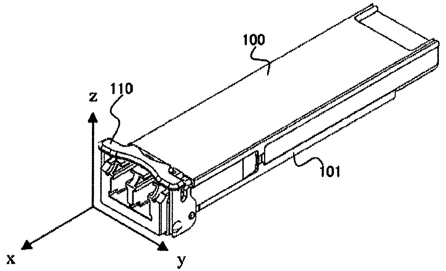
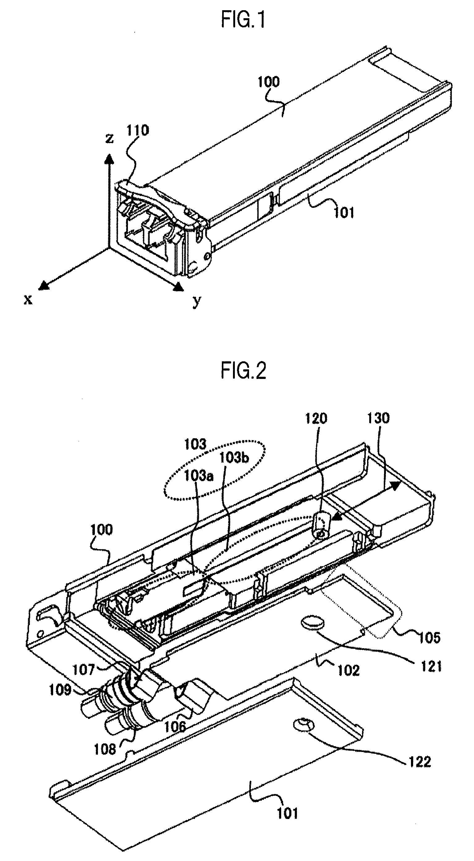
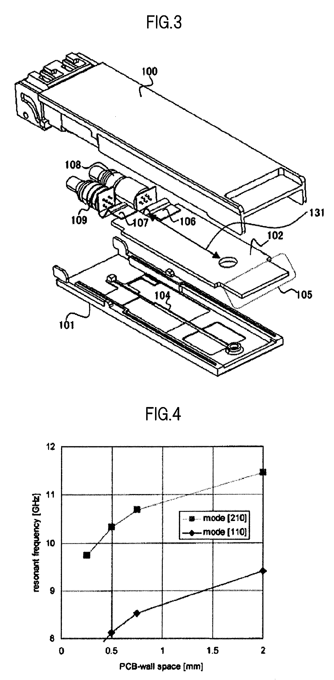
[0038]A first embodiment of the present invention is described with reference to FIGS. 1 to 6. FIG. 1 is a structural view illustrating an appearance of an optical transceiver module according to the first embodiment of the present invention. FIGS. 2 and 3 are exploded perspective views illustrating inner structures of the optical transceiver module according to the first embodiment of the present invention viewed from upper and lower directions. FIG. 4 is a graph showing a change in cavity resonant frequency in an inside of a casing for describing an effect of the first embodiment of the present invention. FIGS. 5 and 6 are graphs showing improvements of a case shield effect for describing an effect of the embodiment of the present invention.

[0039]First, a configuration of the optical transceiver module is described with reference to FIGS. 1 to 3. The optical transceiver module according to the first embodiment is compliant with XFP MSA (SFF Committee INF-8077i, “10 Gigabit Small F...

second embodiment

[0058]A second embodiment of the present invention is described with reference to FIGS. 7 to 9. FIG. 7 is a view illustrating an inner structure of a lower casing according to the second embodiment of the present invention. FIGS. 8 and 9 are graphs showing improvements of a case shield effect for describing an effect of the second embodiment of the present invention. The optical transceiver module according to the second embodiment is also compliant with XFP MSA, but is different from that of the first embodiment, as illustrated in FIG. 7, in that the no partition wall is provided on the lower casing 111 and that the lower casing 111 is formed of a sheet metal product. Similarly to the first embodiment, the partition wall 103 is provided on the upper casing 100 (not shown). As a material for the lower casing 111, a stainless plate, a steel plate, or the like is used.

[0059]FIG. 8 is a graph comparing the case shield effect between a case in which the partition wall is provided in the...

third embodiment

[0062]A third embodiment of the present invention is described with reference to FIGS. 10 to 15. Also in this embodiment, the x-direction is defined as “front”, and the z-direction is defined as “upper”. FIG. 10 is a structural view illustrating an appearance of an optical transceiver module according to the third embodiment of the present invention. FIGS. 11 and 12 are views illustrating inner structures of the upper and lower casing of the optical transceiver module according to the third embodiment of the present invention. FIG. 13 is a view illustrating a positional relationship between the partition walls and the printed circuit board of the optical transceiver module according to the third embodiment of the present invention. FIG. 14 is a graph showing a change in cavity resonant frequency in an inside of a casing for describing an effect of the third embodiment of the present invention. FIG. 15 is a graph showing an improvement of a case shield effect for describing the effec...


PUM


Abstract

Provided is a metal casing structure capable of avoiding a cavity resonance at 10 GHz and 20 GHz by controlling an eigenmode frequency in an inner space of a casing without involving an increase in cost, and a 10 Gbit/s optical transceiver module which achieves reduction in unnecessary electromagnetic waves and cost. In the optical transceiver module, a metal casing having a cavity therein is formed by an upper casing (100) and a lower casing (101), a metal partition wall (103, 104) is provided on at least one of the upper casing (100) and the lower casing (101) near a central portion of the casing in a direction parallel to a direction connecting a front and a rear thereof, and a length of a gap between the partition wall (103, 104) and a printed circuit board (102) is adjusted.

Description

CROSS-REFERENCE TO RELATED APPLICATION[0001]The present application claims priority from Japanese application JP 2007-341375 filed on Dec. 28, 2007, the content of which is hereby incorporated by reference into this application.BACKGROUND OF THE INVENTION[0002]1. Field of the Invention[0003]The present invention relates to an optical transceiver module for optical communication, and more particularly, to a casing structure of a transceiver for optical fiber transmission having a high-speed transmission rate of 10 Gbit / s.[0004]2. Description of the Related Art[0005]A transceiver module for optical fiber transmission (optical transceiver module) is required to achieve a downsizing and higher speed operation in accordance with a widespread use of broadband network in recent years. For the higher speed operation, an optical transceiver module having a bit rate of 10 Gbit / s is now widely used. (For example, there are used ones having 9.95 Gbit / s and 10.7 Gbit / s compliant with Synchronous...

Claims


Application Information

Patent Timeline
IPC IPC(8): H04B10/00H01S5/022
CPCG02B6/4246G02B6/4201G02B6/4277
Inventor KAGAYA, OSAMUISHII, HIROYOSHIKITAJIMA, YASUSHI
Owner LUMENTUM JAPAN INC
Why Eureka
Try Eureka