Radio frequency switch circuit

a frequency switch and circuit technology, applied in the direction of electronic switching, pulse technique, electrical apparatus, etc., can solve the problems of easy and it is not easy to reduce harmonic distortion and higher-order intermodulation distortion

Inactive Publication Date: 2009-07-16
KK TOSHIBA
View PDF3 Cites 77 Cited by
  • Summary
  • Abstract
  • Description
  • Claims
  • Application Information

AI Technical Summary

Problems solved by technology

This off-state of n-stage series connected transistors is likely to cause harmonic distortion and higher-order intermodulation distortion based on the nonlinearity of off-capacitance with respect to voltage.
However, even if this technique is used, it is not easy to reduce harmonic distortion and higher-order intermodulation distortion to meet the requirements of GSM and UMTS without increasing the chip size of the radio frequency switch circuit.

Method used


Image

  • Radio frequency switch circuit
  • Radio frequency switch circuit
  • Radio frequency switch circuit

Examples


first embodiment

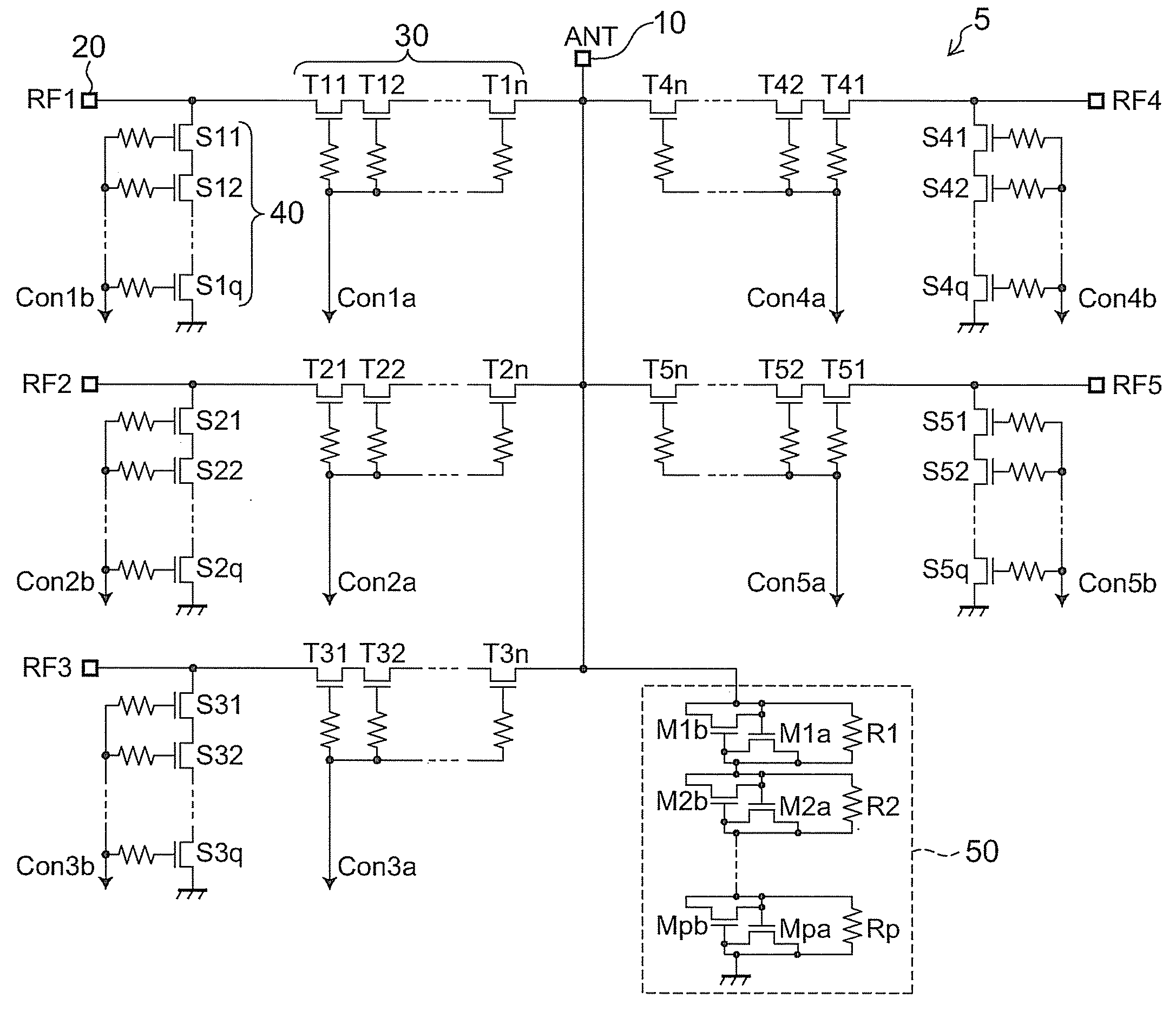
[0036]FIG. 1 shows a radio frequency switch circuit according to the invention. This embodiment illustrates the configuration of an SP5T switch, which can switch the state of conduction (electrical connection) between an antenna terminal 10 and five radio frequency (hereinafter RF) terminals by controlling FETs. Transceiver circuits are connected to at least two RF terminals.

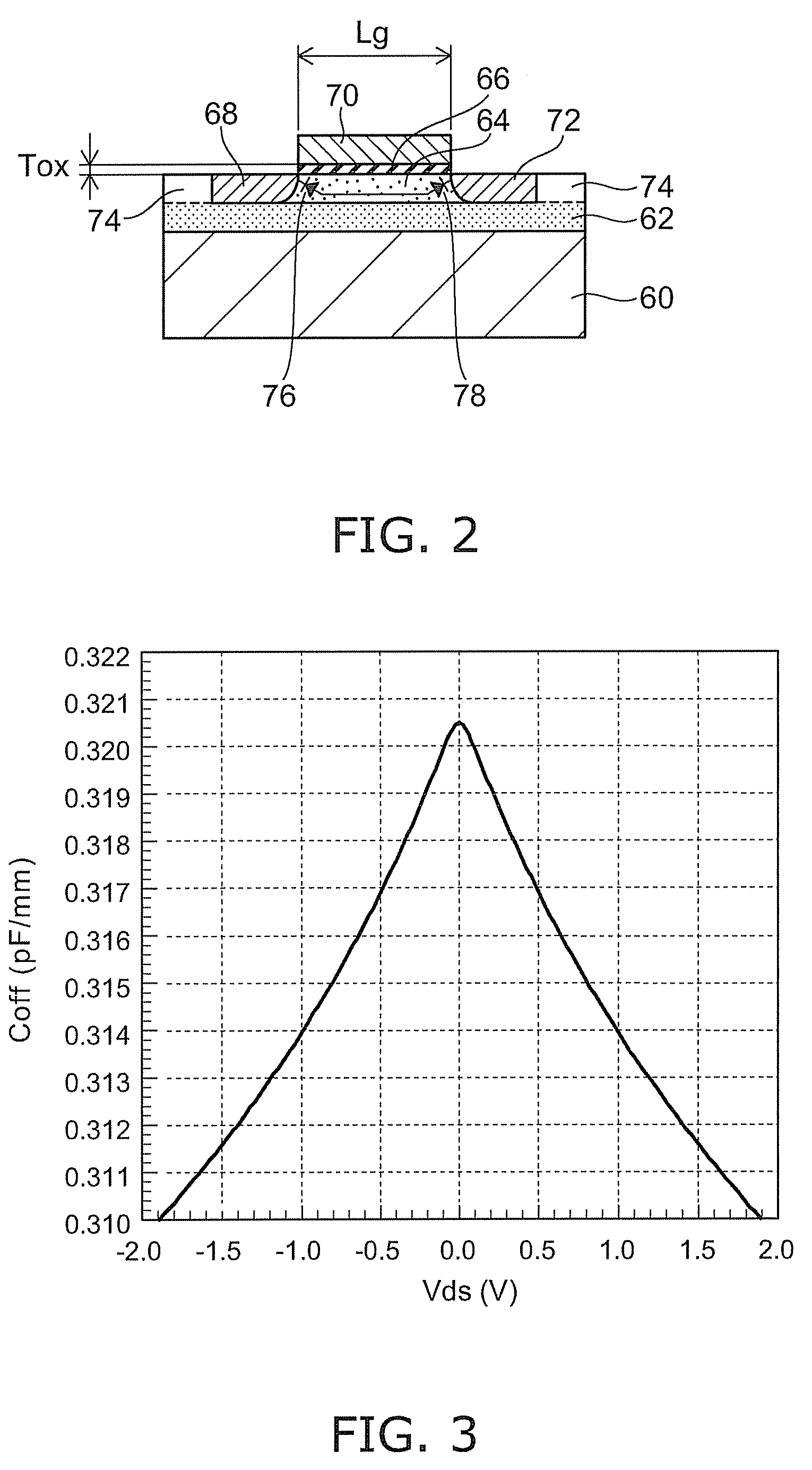
[0037]In this embodiment, a distortion compensation circuit 50 is placed between the antenna terminal 10 and the ground. The distortion compensation circuit 50 is composed of a reverse connected MOS capacitor and compensates for nonlinear distortion based on the voltage dependence of off-capacitance Coff in the off-state of FETs. The distortion compensation circuit 50 is described later in detail.

[0038]In this example, through FETs (through transistors) 30 placed between the antenna terminal 10 and the first RF terminal (hereinafter RF1 terminal) 20 are turned on, shunt FETs (shunt transistors) 40 placed between...

third embodiment

[0077]It is noted that the distortion compensation circuit 50, 51 is not limited to the first to The gate width Wg and the threshold voltage Vth of the MOSFET constituting the distortion compensation circuit 50, 51 can be varied, and the distortion compensation circuit 50, 51 can be suitably placed at one or more of the antenna terminal 10 and the RF terminals.

[0078]FIG. 13 is a configuration view of a radio frequency section of a mobile phone including the radio frequency switch circuit of this embodiment. An antenna 90 is connected to the antenna terminal 10 of the radio frequency switch circuit 5 including the distortion compensation circuit 50. An output terminal of a transmit amplifier 92a of a GSM low-band (900 MHz band) transceiver circuit 92 is connected to the RF1 terminal, and an input terminal of a receive amplifier 92b thereof is connected to the RF2 terminal. An output terminal of a transmit amplifier 94a of a GSM high-band (1800 MHz band) transceiver circuit 94 is con...

fourth embodiment

[0080]FIG. 14 illustrates a radio frequency switch circuit according to a More specifically, FIG. 14A is a connection diagram of a transistor and MOS capacitors, and FIG. 14B shows the drain-source voltage dependence of terminal-to-terminal capacitance. The vertical axis represents capacitance (pF), and the horizontal axis represents the drain-source voltage Vds (V).

[0081]A transistor ST and a distortion compensation circuit 52 are parallel connected between the terminal P4 and the terminal Q4. The distortion compensation circuit 52 includes a first MOS capacitor 52a in which MOSFETs having a MOS capacitance are parallel connected to each other in reverse direction, and a second MOS capacitor 52b in which MOSFETs are parallel connected to each other in reverse direction. The transistor ST is series connected and illustratively constitutes the through transistor Tij and the shunt transistor Sij.

[0082]If the transistor ST is an N-channel MOSFET, its threshold voltage Vth can be set t...


PUM


Abstract

A radio frequency switch circuit includes: an antenna terminal; a first and second RF terminal; a first through transistor placed between the antenna terminal and the first RF terminal; a second through transistor placed between the antenna terminal and the second RF terminal; a first shunt transistor placed between ground and the first RF terminal; a second shunt transistor placed between the ground and the second RF terminal; and a distortion compensation circuit including a reverse parallel connected MOS capacitor whose capacitance around 0 volts has voltage dependence that is convex to the minus direction, the distortion compensation circuit being operable to compensate for voltage dependence of off-capacitance around 0 volts of the first and second through transistor and the first and second shunt transistor that is convex to the plus direction. Electrical connection between the antenna terminal and the first and second RF terminal is switchable.

Description

CROSS-REFERENCE TO RELATED APPLICATIONS[0001]This application is based upon and claims the benefit of priority from the prior Japanese Patent Application No. 2008-005681, filed on Jan. 15, 2008 and the prior Japanese Patent Application No. 2008-246660, filed on Sep. 25, 2008; the entire contents of which are incorporated herein by reference.BACKGROUND OF THE INVENTION[0002]1. Field of the Invention[0003]This invention relates to a radio frequency switch circuit.[0004]2. Background Art[0005]A multi-port radio frequency switch circuit such as an SP5T (single-pole 5-throw) switch is used in multi-mode multi-band wireless equipment. In this case, multi-stage series connected through FETs are provided between an antenna terminal and five RF terminals, and multi-stage series connected shunt FETs are provided between each RF terminal and the ground.[0006]For example, for conduction between the first RF terminal and the antenna terminal, the through FETs and shunt FETs are controlled as fol...

Claims


Application Information

Patent Timeline
Patent Type & Authority Applications(United States)
IPC IPC(8): H04B1/18
CPCH04B1/48H04B1/006H03K17/693
Inventor SESHITA, TOSHIKISAGAE, YOSHITOMO
Owner KK TOSHIBA
Why Eureka
Try Eureka