Solid-state imaging device, manufacturing method for the same, and imaging apparatus

a solid-state imaging and manufacturing method technology, applied in the direction of color television, television systems, radio control devices, etc., can solve the problems of deterioration of photoelectric conversion characteristics, difficulty in achieving both the realization of a sufficient hole accumulation layer and a reduction of dark current, etc., to reduce the generation of white dots, reduce the generation of noise in picked-up images, and improve the effect of image quality

Active Publication Date: 2009-07-30
SONY CORP
View PDF2 Cites 43 Cited by
  • Summary
  • Abstract
  • Description
  • Claims
  • Application Information

AI Technical Summary

Benefits of technology

[0022]In the first solid-state imaging device, since the film having negative fixed charges is formed on the film for reducing interface state density, the hole accumulation layer is sufficiently formed in an interface on the light-receiving surface side of the light-receiving section by an electric field due to the negative fixed charges. Therefore, the generation of charges (electrons) from the interface is suppressed. Even if charges (electrons) are generated, since the charges flows in the hole accumulation layer in which a large number of holes are present without flowing into a charge accumulation portion forming a well of potential in the light-receiving section, the charges (the electrons) can be eliminated. Therefore, it is possible to prevent the charges due to the interface from changing to dark currents to be detected by the light-receiving section and suppress the dark currents due to the interface state density. Moreover, since the film for reducing interface state density is formed on the light-receiving surface of the light-receiving section, the generation of electrons due to the interface state density is further suppressed. Therefore, the electrons due to the interface state density are prevented from flowing into the light-receiving section as dark currents.
[0041]With the imaging apparatus according to the embodiments, since the solid-state imaging devices that can suppress dark current are used, noise in a picked-up image can be reduced. Therefore, there is an effect that it is possible to record a high-definition video. In particular, it is possible to reduce generation of white dots (dots of the primary colors in a color CCD) due to dark currents in long-time exposure with a small exposure amount.

Problems solved by technology

When it is attempted to form a sufficient hole accumulation layer by implanting ions into a light-receiving section (a photoelectric conversion section) at high density, since the light-receiving section is damaged by the ion implantation, annealing at high temperature is necessary but, in the annealing, spread of impurities occurs and a photoelectric conversion characteristic is deteriorated.
The hole accumulation layer does not have a sufficient function of the hole accumulation layer.
In other words, it is difficult to achieve both the realization of a sufficient hole accumulation layer and a reduction in dark currents while suppressing the spread of impurities and having a desired photoelectric conversion characteristic.

Method used


Image

  • Solid-state imaging device, manufacturing method for the same, and imaging apparatus
  • Solid-state imaging device, manufacturing method for the same, and imaging apparatus
  • Solid-state imaging device, manufacturing method for the same, and imaging apparatus

Examples


first embodiment

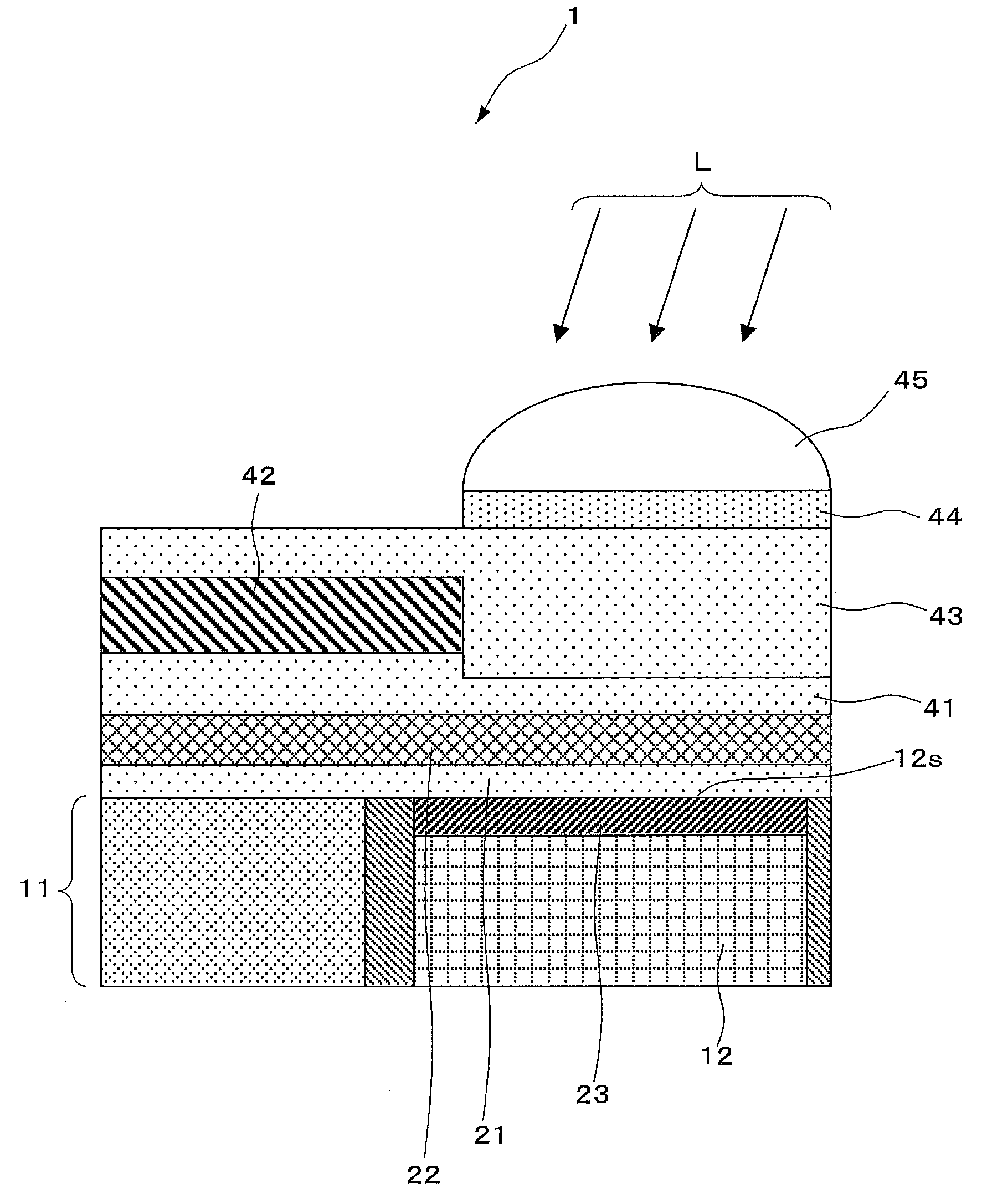
[0096]A solid-state imaging device (a first solid-state imaging device) according to the present invention is explained below with reference to a sectional view of a main part configuration in FIG. 1.

[0097]As shown in FIG. 1, the solid-state imaging device 1 has, in a semiconductor substrate (or a semiconductor layer) 11, a light-emitting section 12 that photoelectrically converts incident light L. The solid-state imaging device 1 has, on a side of the light-receiving section 12, a peripheral circuit section 14 in which peripheral circuits (not specifically shown) are formed via a pixel separation area 13.

[0098]In the following explanation, the solid-state imaging device 1 has the light-receiving section 12 in the semiconductor substrate 11.

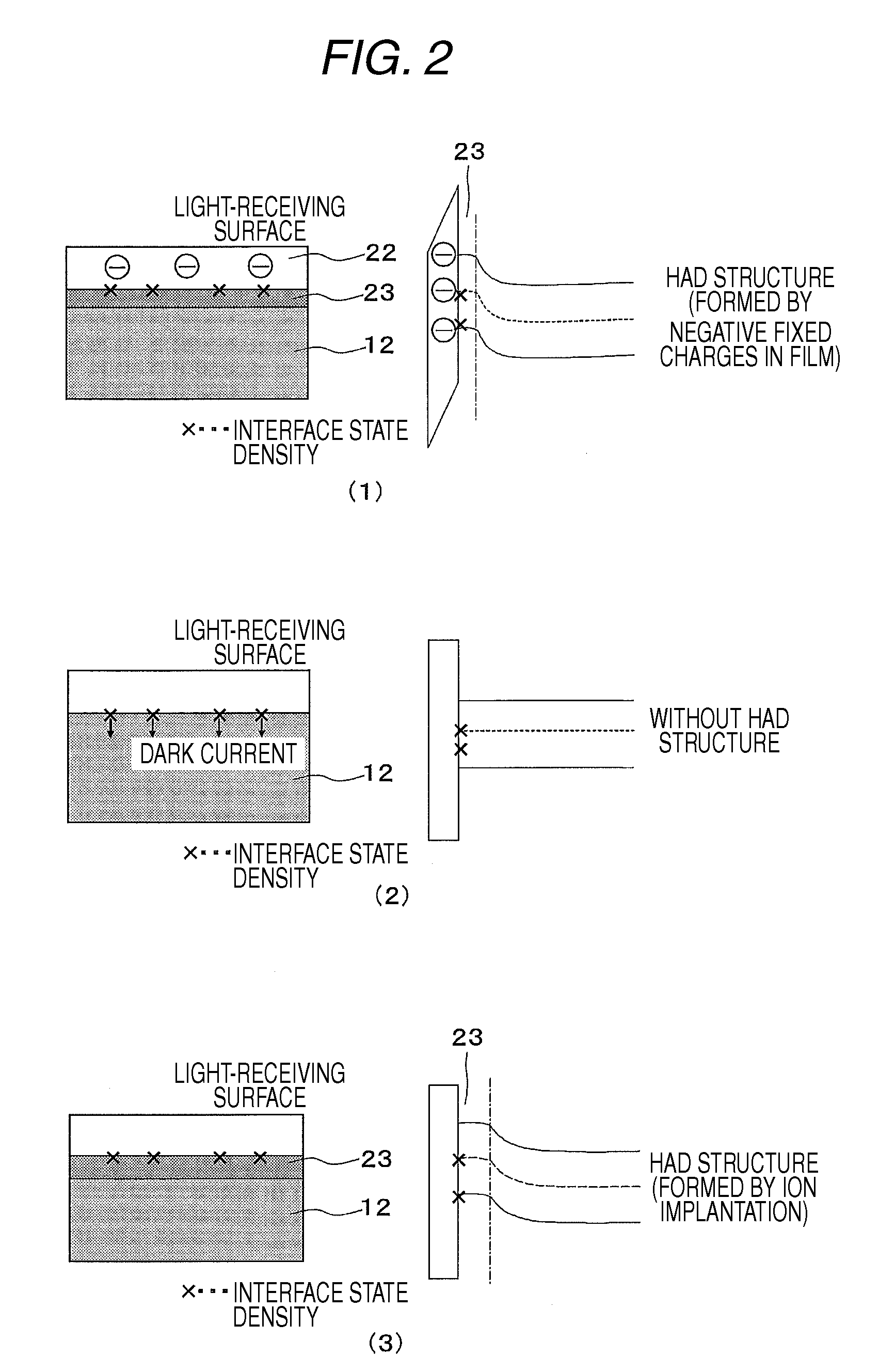
[0099]A film 21 for reducing interface state density is formed on a light-receiving surface 12s of the light-receiving section (including a hole accumulation layer 23 described later) 12. The film 21 for reducing interface state density is formed...

second embodiment

[0135]A solid-state imaging device (a first solid-state imaging device) according to the present invention is explained with reference to a sectional view of a main part configuration in FIG. 6.

[0136]In FIG. 6, a light shielding film that shields a part of a light-receiving section and a peripheral circuit section, a color filter layer that splits light made incident on the light-receiving section, a condensing lens that condenses the incident light on the light-receiving section, and the like are not shown.

[0137]As shown in FIG. 6, in a solid-state imaging device 4, an insulating film 24 is formed between the surface of the peripheral circuit section 14 and the film 22 having negative fixed charges such that a distance from the surface of the peripheral circuit section 14 to the film 22 is larger than a distance from the surfaces of the light-receiving sections 12 to the film 22 in the solid-state imaging device 1. When the film for reducing interface state density is formed by a s...

third embodiment

[0140]A solid-state imaging device (a first solid-state imaging device) according to the present invention is explained with reference to a sectional view of a main part configuration in FIG. 7.

[0141]In FIG. 7, a light shielding film that shields a part of a light-receiving section and a peripheral circuit section, a color filter layer that splits light made incident on the light-receiving section, a condensing lens that condenses the incident light on the light-receiving section, and the like are not shown.

[0142]As shown in FIG. 7, in a solid-state imaging device 5, a film 25 for separating a film having negative fixed charges and a light-receiving surface is formed between the peripheral circuit section 14 and the film 22 having negative fixed charges in the solid-state imaging device 1. The film 25 desirably has positive fixed charges to cancel the influence of the negative fixed charges. For example, silicon nitride is preferably used for the film 25.

[0143]In this way, the film ...


PUM


Abstract

A solid-state imaging device having a light-receiving section that photoelectrically converts incident light includes an insulating film formed on a light-receiving surface of the light-receiving section and a film and having negative fixed charges formed on the insulating film. A hole accumulation layer is formed on a light-receiving surface side of the light-receiving section. A peripheral circuit section in which peripheral circuits are formed is provided on a side of the light-receiving section. The insulating film is formed between a surface of the peripheral circuit section and the film having negative fixed charges such that a distance from the surface of the peripheral circuit section to the film having negative fixed charges is larger than a distance from a surface of the light-receiving section to the film having negative fixed charges.

Description

CROSS-REFERENCES TO RELATED APPLICATIONS[0001]The present invention contains subject matter related filed in the Japanese Patent Office on May 7, 2007 and Dec. 26, 2007, respectively, the entire contents of which being incorporated herein by reference.BACKGROUND OF THE INVENTION[0002]1. Field of the Invention[0003]The present invention relates to a solid-state imaging device with the generation of dark currents suppressed, a manufacturing method for the solid-state imaging device, and an imaging apparatus.[0004]2. Description of the Related Art[0005]In video cameras and digital still cameras, solid-state imaging devices including CCD (Charge Coupled Device) or CMOS image sensors are widely used. A reduction in noise as well as improvement of sensitivity is an important object for all the solid-stage imaging devices.[0006]Regardless of a state in which there is no incident light, i.e., a state in which there is no pure signal charge generated by photoelectric conversion of incident l...

Claims


Application Information

Patent Timeline
Patent Type & Authority Applications(United States)
IPC IPC(8): H01L31/10H01L31/18H01L31/0232H01L27/146H01L27/148H01L31/00H04N5/335H04N5/361H04N5/369
CPCH01L27/1461H01L27/1462H01L27/14629H01L27/14643H01L27/14683H01L27/1464H01L27/14621H01L27/14623H01L27/14625H01L27/14627H01L27/14636H01L27/14645H01L27/14818H01L27/14868H01L27/148H01L31/10
Inventor IKEDA, HARUMIHIYAMA, SUSUMUANDO, TAKASHITABUCHI, KIYOTAKAYAMAGUCHI, TETSUJIOHGISHI, YUKO
Owner SONY CORP
Why Eureka
Try Eureka