Display driving device, display apparatus, and method of driving them
a technology of display device and display device, which is applied in the direction of instruments, computing, electric digital data processing, etc., can solve the problems of increasing the circuit size of the display device, and achieve the effect of reducing the circuit size and favorable display of image information
- Summary
- Abstract
- Description
- Claims
- Application Information
AI Technical Summary
Benefits of technology
Problems solved by technology
Method used
Image
Examples
first embodiment
[0054]First, the schematic configuration of a display apparatus according to the invention will be described with reference to the drawings.
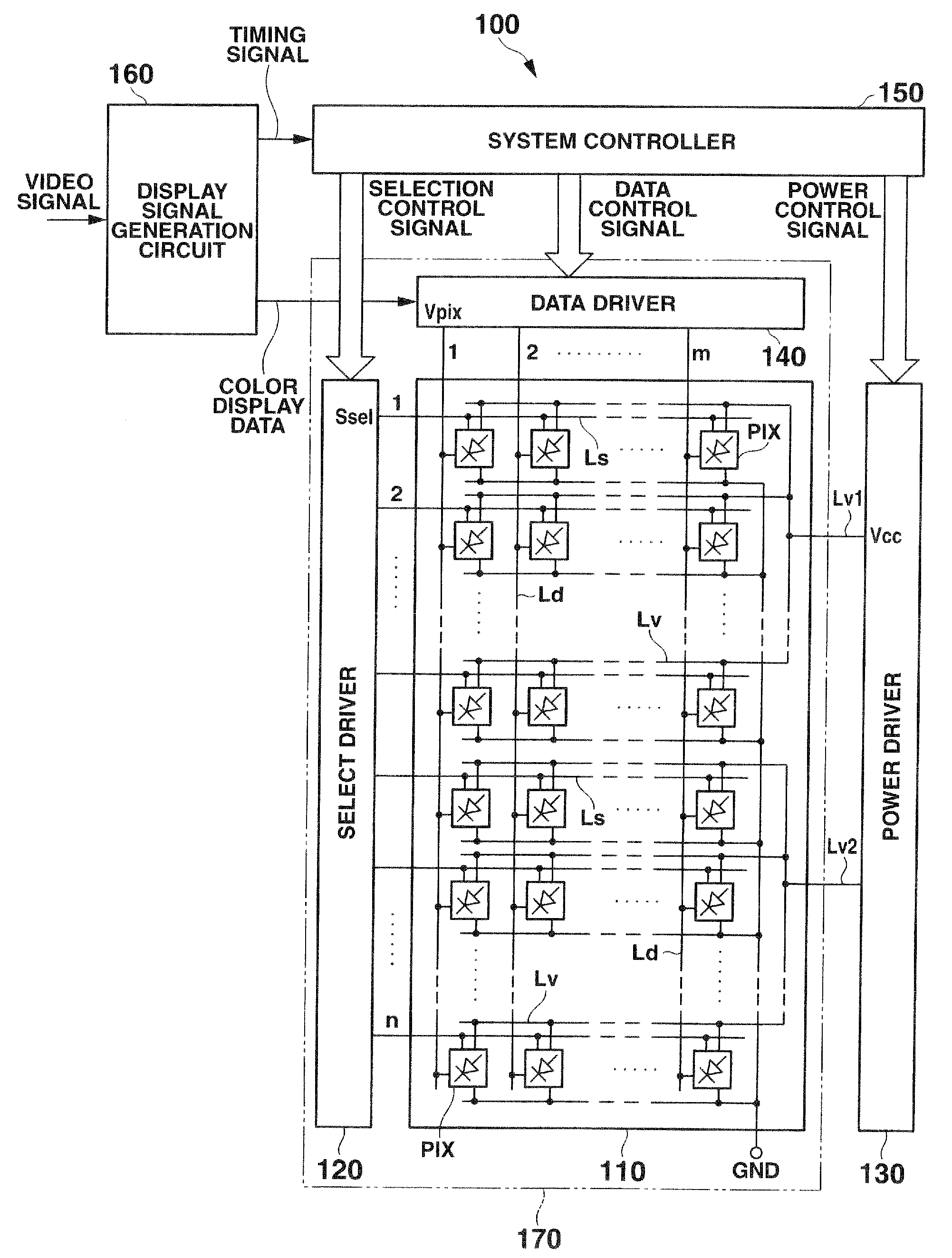
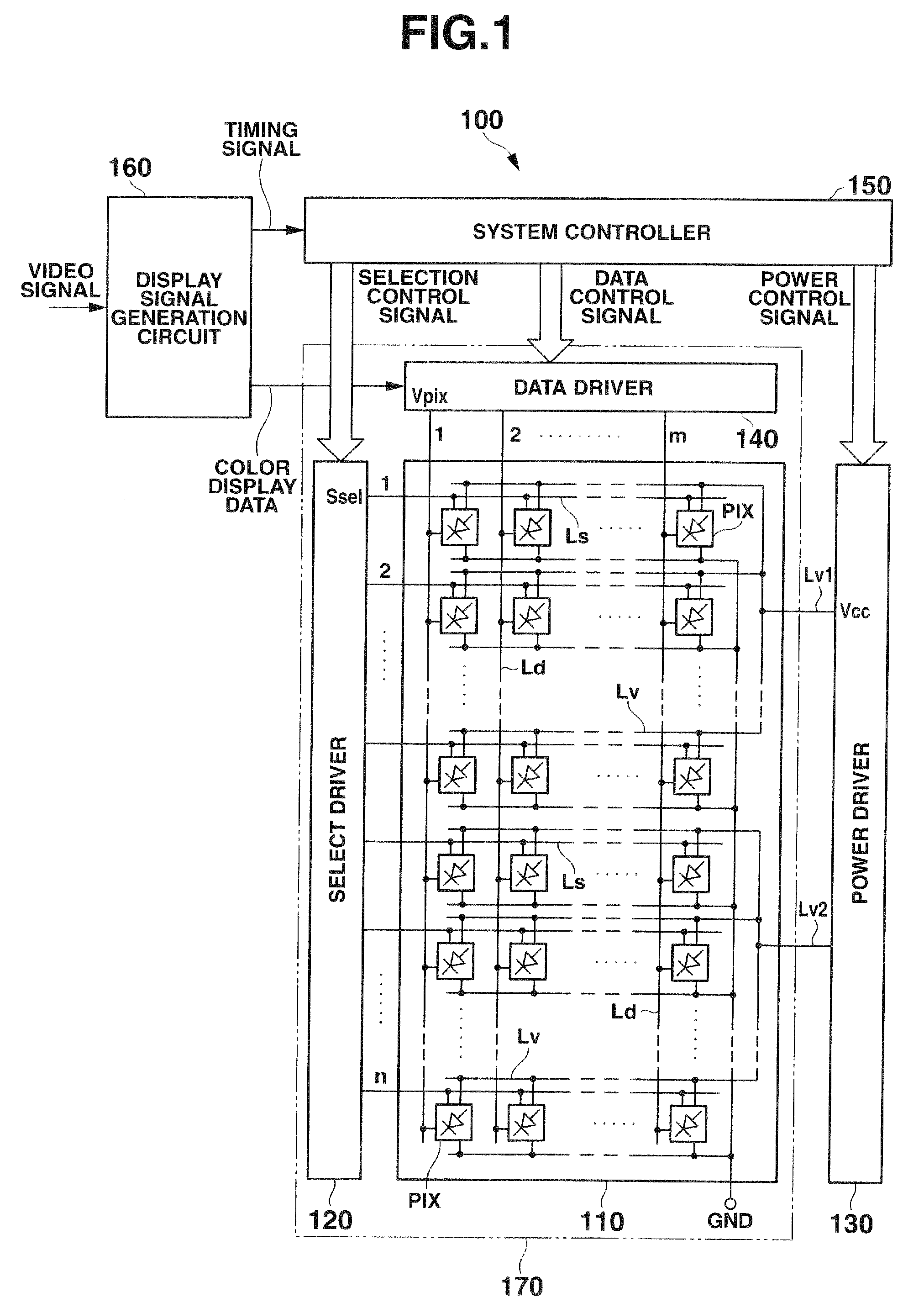
[0055]FIG. 1 is a schematic block diagram showing an example of the entire configuration of the display apparatus according to the invention.
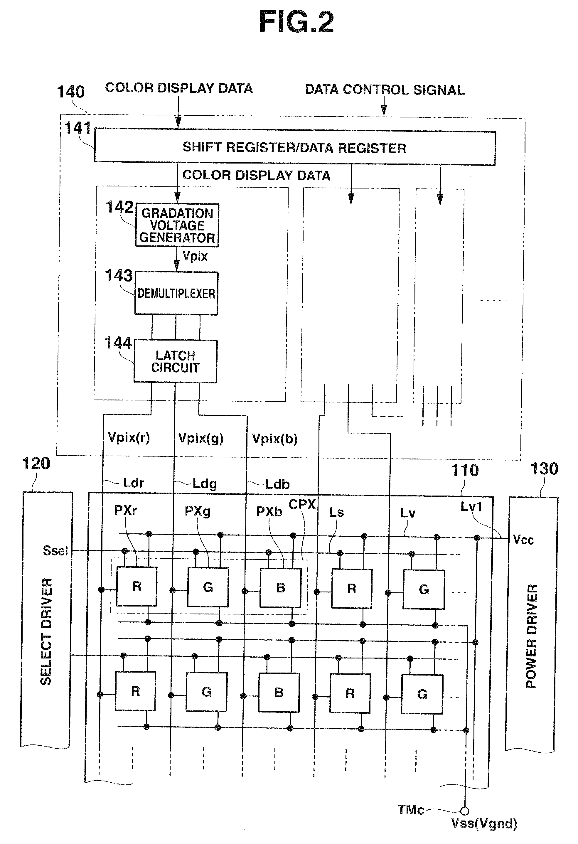
[0056]FIG. 2 is a schematic configuration diagram showing an example of a display panel and a data driver applicable to the display apparatus according to a first embodiment.
[0057]As shown in FIG. 1, a display apparatus 100 according to the present embodiment is provided with a display panel 170 constituted of a substrate having a display area 110, a select driver 120, and a data driver 140 provided thereon, a power driver 130, a system controller 150, and a display signal generation circuit 160.
[0058]The display area 110 has, for example, a plurality of select lines Ls arranged in a row direction (horizontal direction in the drawing), a plurality of data lines Ld arranged in a column direction (vertical di...
second embodiment
[0202]Next, a second embodiment according to the invention will be described. The entire constitution of the display apparatus in the second embodiment is equivalent to that in the first embodiment, and therefore, in the following description, there will be described in detail the constitution of the data driver and the driving method specific to the second embodiment.
[0203]In the first embodiment, in accordance with the timing at which the display data of each color of R, G, and B (luminance gradation value) is sequentially supplied to the data driver 140 (gradation voltage generator 142), the maximum luminance reference voltages Vmax(R), Vmax(G), and Vmax(B) and the minimum luminance reference voltages Vs(R), Vc(G), and Vs(B) are switched and set so that the characteristics of the gamma correction curve in the γ curve generation circuit (gamma correction circuit) 142-1 are corresponded to the electro-optic characteristics of the organic EL element OLED of each color of R, G, and B...
third embodiment
[0210]In the first embodiment, the characteristics of the gamma correction curve in the γ curve generation circuit (gamma correction circuit) 142-1 are switched corresponding to the display data (luminance gradation value) of each color or R, G, and B sequentially supplied to the data driver 140 (gradation voltage generator 142), and the gradation voltages Vpix (Vpix(r), Vpix(g), and Vpix(b)) corresponding to the electro-optic characteristics of the organic EL element OLED of each color of R, G, and B are generated. Thereafter, the gradation voltages Vpix are distributed in a time sharing manner by the demultiplexer 143 so as to correspond to each color of R, G, and B, and further temporarily held in the latch circuit 144 to be simultaneously applied to the display pixels PIX (sub pixels PXr, PXg, and PXb) of each color of R, G, and B at a predetermined timing, and thus, to be written in the display pixels PIX.
[0211]In contrast, in the third embodiment, the gradation voltages Vpix (...
PUM
 Abstract
Description
Claims
Application Information


