Hardmask open process with enhanced CD space shrink and reduction

a technology of shrinkage and reduction, which is applied in the direction of photosensitive material processing, photomechanical equipment, instruments, etc., can solve the problems of anisotropic striation formation, insufficient process to produce small geometry, and difficulty in precise critical dimension and etch profile control

Inactive Publication Date: 2009-07-30
APPLIED MATERIALS INC
View PDF12 Cites 205 Cited by
  • Summary
  • Abstract
  • Description
  • Claims
  • Application Information

AI Technical Summary

Benefits of technology

[0009]Embodiments of the invention include forming small dimensional structures on a substrate using a method that includes multiple processes of polymer deposition and etching. The structures formed on the substrate include vias, trenches, holes, patterned features, and the like. The embodiments described herein may be advantageously utilized to fabricate a submicron structures on a substrate having critical dimensions less than 55 nm and are particularly suitable for dual damascene applications.

Problems solved by technology

Reliably producing sub-half micron and smaller features is one of the key technology challenges for next generation very large scale integration (VLSI) and ultra large-scale integration (ULSI) of semiconductor devices.
However, as the limits of circuit technology are pushed, the shrinking dimensions of VLSI and ULSI interconnect technology have placed additional demands on processing capabilities.
However, with shrinking geometries, precise critical dimension and etch profile control has become increasingly difficult.
Especially for via fabrication, many processes are inadequate to produce smaller geometry and are limited to about 50 nm to 60 nm in critical dimensions (CD) which are larger than desired and therefore must rely on etch processes to shrink CD during a bottom anti-reflective coating (BARC) and / or an anti-reflective coating (ARC) open process.
Another problem found during submicron 55 nm plasma etching processes is control of the sidewall roughness of the etched structure, which may result in formation of anisotropic striation.
As the dimensions of the features continue to diminish, the occurrence of sidewall striation and / or post-etch sidewall roughness occurrence in small critical dimension structures pose a significant challenge to structure profile integrity, especially when significant critical dimensions (CD) shrinkage is required during a bottom anti-reflective coating (BARC) and / or an anti-reflective coating (ARC), which may ultimately deteriorate overall device performance.
Furthermore, the conventional lithography technique, e.g., utilizing 193 nm ArF as light source, tends to have resolution limitation on photoresist layers having a thickness greater than 2000 Å. Similarity of each materials, such as a bottom anti-reflective coating (BARC) and / or an anti-reflective coating (ARC) and a photoresist layer, results in similar etch properties therebetween, thereby causing poor selectivity.
Poor etching selectivity may result in poor structure integrity, such as non-uniformity or tapered profile formed on the top and / or sidewall of the formed structure on the substrate, thereby eventually leading to device failure.

Method used


Image

  • Hardmask open process with enhanced CD space shrink and reduction
  • Hardmask open process with enhanced CD space shrink and reduction
  • Hardmask open process with enhanced CD space shrink and reduction

Examples


Embodiment Construction

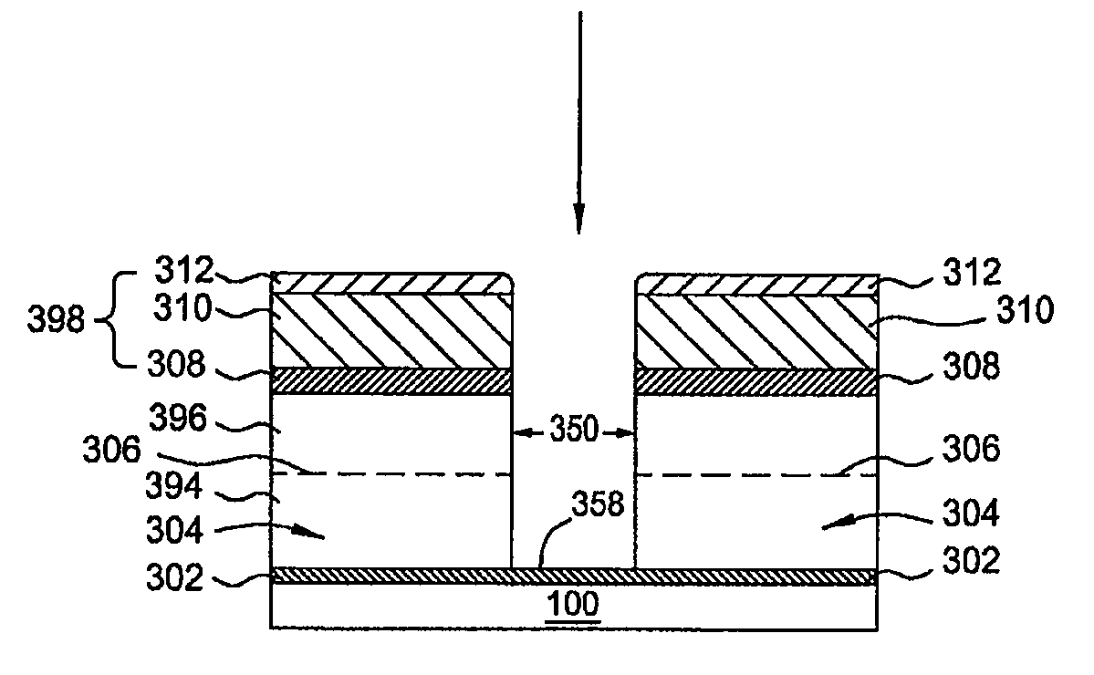
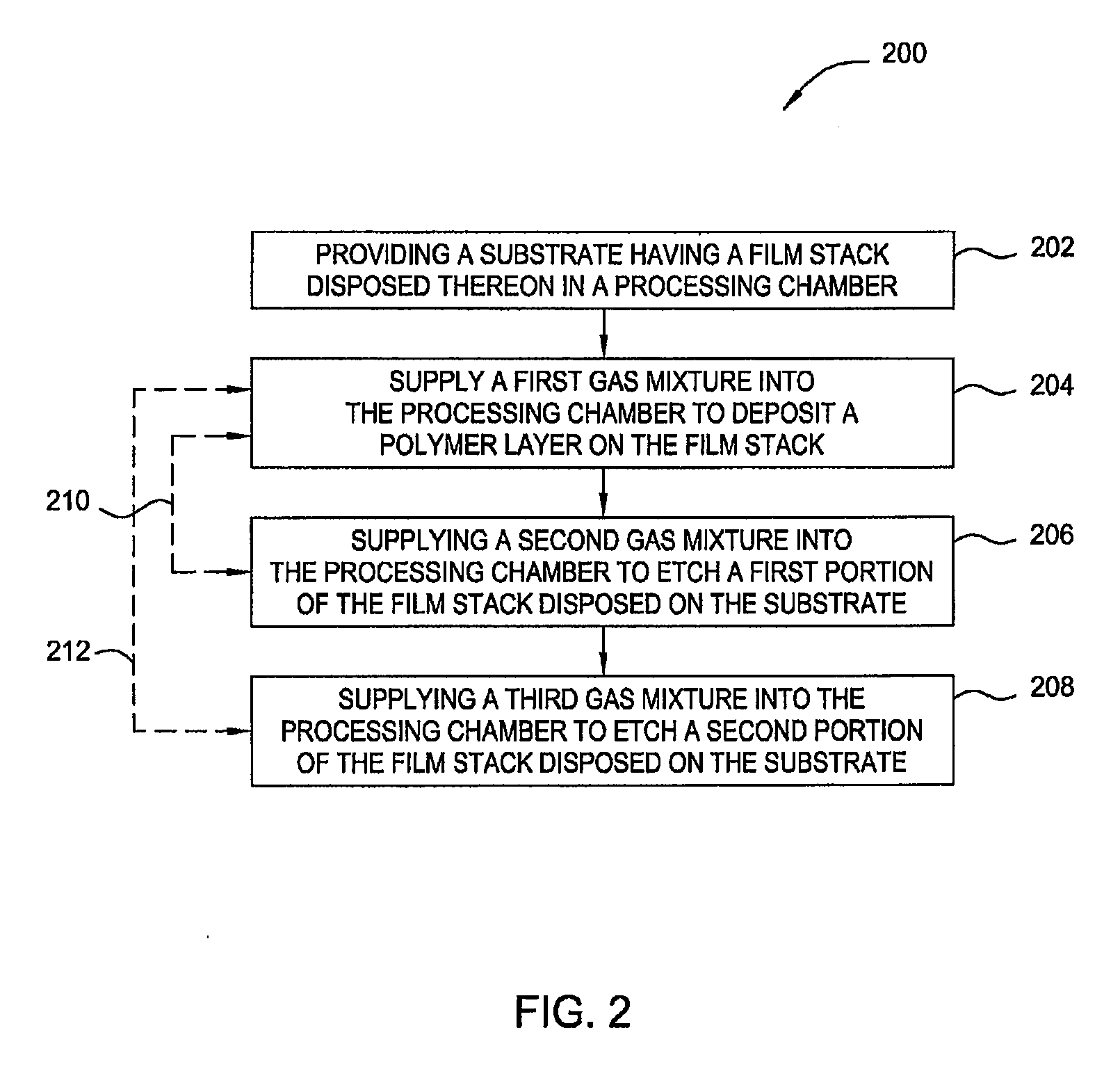
[0021]Embodiments of the invention generally relate to methods for forming structures on a substrate substantially without sidewall striation and critical dimension loss. The structures formed in the substrate include vias, trenches, holes, patterned features, and the like. In one embodiment, the structures having a critical dimension down to 55 nm or less are formed using multiple processes of polymer deposition and etching process. The method is particularly suitable for etching a bottom anti-refectory coating (BARC) layer (or called anti-refectory coating (ARC) layer) and / or a hardmask layer which is later utilized as a mask layer to etch a dielectric layer as part of a dual damascene fabrication process. The method described herein includes a polymer deposition process and followed by multiple etching process to gradually etch the layers and shrink critical dimension of the structures formed in the layer while maintaining control of structure profile and geometry. By utilizing m...


PUM

PropertyMeasurementUnit
roughnessaaaaaaaaaa
thicknessaaaaaaaaaa
frequencyaaaaaaaaaa

Abstract

Methods for forming an ultra thin structure. The method includes a polymer deposition and etching process. In one embodiment, the methods may be utilized to form fabricate submicron structure having a critical dimension less than 30 nm and beyond. The method further includes a multiple etching processes. The processes may be varied to meet different process requirements. In one embodiment, the process gently etches the substrate while shrinking critical dimension of the structures formed within the substrate. The dimension of the structures may be shank by coating a photoresist like polymer to sidewalls of the formed structure, but substantially no polymer accumulation on the bottom surface of the formed structure on the substrate. The embodiments described herein also provide high selectivity in between each layers formed on the substrate during the fabricating process and preserving a good control of profile formed within the structure.

Description

BACKGROUND[0001]1. Field[0002]Embodiments of the present invention generally relates to methods for forming structures on a substrate, and more specifically, for using multiple etching and polymer deposition processes to form structures on a substrate in dual damascene applications.[0003]2. Description of the Related Art[0004]Reliably producing sub-half micron and smaller features is one of the key technology challenges for next generation very large scale integration (VLSI) and ultra large-scale integration (ULSI) of semiconductor devices. However, as the limits of circuit technology are pushed, the shrinking dimensions of VLSI and ULSI interconnect technology have placed additional demands on processing capabilities. Reliable formation of structures accurately formed on the substrate is important to VLSI and ULSI success and to the continued effort to increase circuit density and quality of individual substrates and die.[0005]A patterned mask is commonly used in forming structures...

Claims


Application Information

Patent Timeline
Patent Type & Authority Applications(United States)
IPC IPC(8): H01L21/306C23F1/08
CPCG03F7/091G03F7/40H01J37/32091H01J37/3244H01J37/3266H01L21/76802H01L21/0338H01L21/31116H01L21/31138H01L21/31144H01L21/0337
Inventor RUI, YINGFUNG, NANCYZHAO, XIAOYEMUKAI, KEVIN MIKIOIWAMOTO, YASUNOBU
Owner APPLIED MATERIALS INC
Why Eureka
Try Eureka