Semiconductor device having wiring line and manufacturing method thereof

a technology of semiconductor devices and wiring lines, which is applied in the direction of semiconductor devices, semiconductor/solid-state device details, electrical apparatus, etc., can solve the problems of limited miniaturization of semiconductor constructs and inability to increase the number of columnar electrodes, and achieve the effect of further miniaturization

Inactive Publication Date: 2009-08-06
TERAMIKROS INC
View PDF17 Cites 8 Cited by
  • Summary
  • Abstract
  • Description
  • Claims
  • Application Information

AI Technical Summary

Benefits of technology

[0008]It is therefore an object of this invention to provide a semiconductor device and a manufacturing method thereof that enable further miniaturization.

Problems solved by technology

Therefore, there has been a problem that the miniaturization of the semiconductor construct is limited and an increase in the number of columnar electrodes is not possible.

Method used


Image

  • Semiconductor device having wiring line and manufacturing method thereof
  • Semiconductor device having wiring line and manufacturing method thereof
  • Semiconductor device having wiring line and manufacturing method thereof

Examples


first embodiment

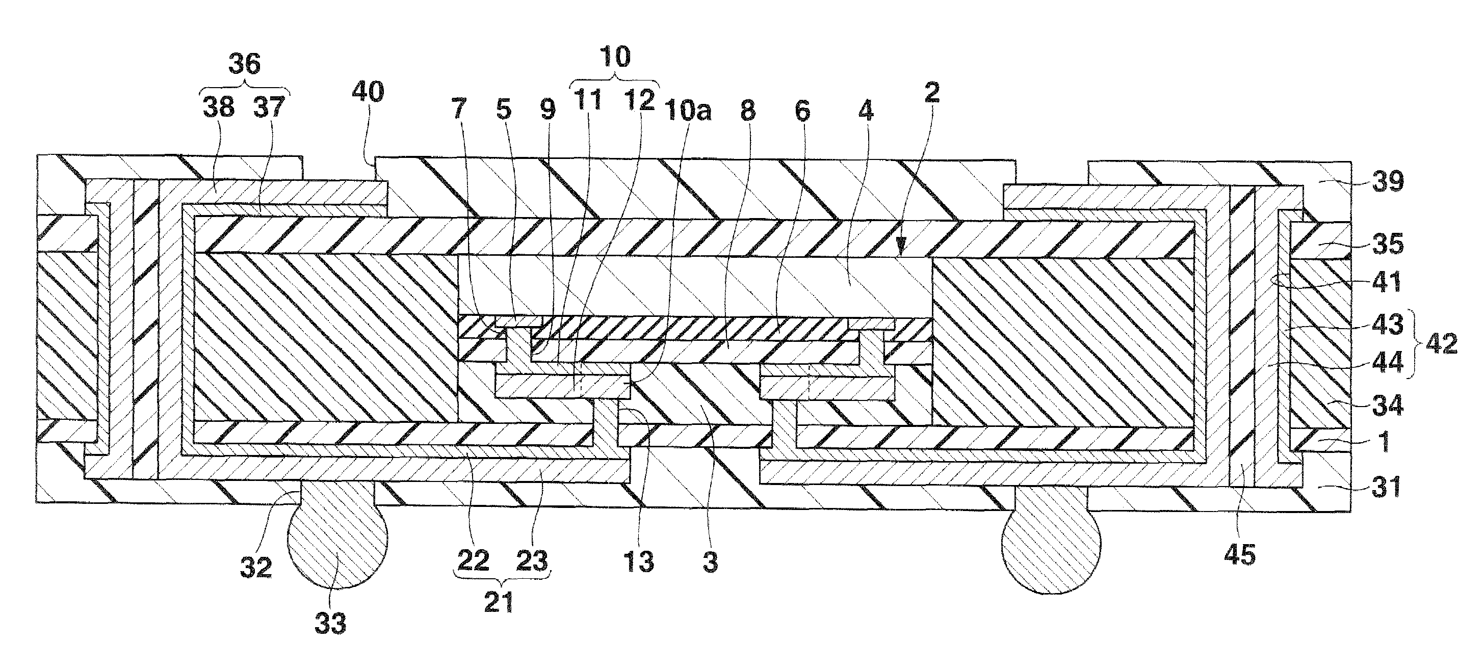
[0050]FIG. 1 shows a sectional view of a semiconductor device as a first embodiment of this invention. This semiconductor device comprises a planar square lower insulating film 1 made of, for example, an epoxy resin, a polyimide resin, or an epoxy resin having a glass cloth base material. A semiconductor construct 2 is installed at the center of the upper surface of the lower insulating film 1 via an adhesive layer 3 made of, for example, an epoxy resin.

[0051]The semiconductor construct 2 comprises a planar square silicon substrate (semiconductor substrate) 4. An integrated circuit (not shown) having a predetermined function is provided on the lower surface of the silicon substrate 4. In the peripheral parts of this lower surface, a plurality of connection pads 5 made of, for example, an aluminum-based metal and connected to the integrated circuit are provided along the sides of the silicon substrate. An insulating film 6 made of, for example, silicon oxide is provided on the lower ...

second embodiment

[0081]FIG. 14 shows a sectional view of a semiconductor device as a second embodiment of this invention. This semiconductor device is different from the semiconductor device shown in FIG. 1 in that a lower metal layer 61 made of copper is provided between a lower wiring line 21 and a lower insulating film 1, in that a lower metal layer 62 made of copper is provided between an upper wiring line 36 and an upper insulating film 35, and in that the upper surface of a silicon substrate 4 of a semiconductor construct 2 is adhesively bonded to the lower surface of the upper insulating film 35 via an adhesive layer 63 made of, for example, an epoxy resin. In this case, one end of the lower wiring line 21 is connected to a connection pad portion 10a of a wiring line 10 of the semiconductor construct 2 via an opening 64 of the lower metal layer 61 and an opening 13 of an adhesive layer 3 and the lower insulating film 21.

[0082]Next, one example of a method of manufacturing this semiconductor d...

third embodiment

[0090]FIG. 23 shows a sectional view of a semiconductor device as a third embodiment of this invention. This semiconductor device is greatly different from the semiconductor device shown in FIG. 1 in that both a lower wiring line and an upper wiring line are formed to have a double-layer wiring structure by use of a build-up method. That is, a second lower insulating film 1B made of the same material as a first lower insulating film 1A is provided on the lower surface of the first lower insulating film 1A including a first lower wiring line 21A and a lower wiring line 21.

[0091]One end of a second lower wiring line 21B provided on the lower surface of the second lower insulating film 1B is connected to the connection pad portion of the first lower wiring line 21A via an opening 71 provided in the second lower insulating film 1B. A lower overcoat film 31 is provided on the lower surface of the second lower insulating film 1B including the second lower wiring line 21B. A solder ball 33...


PUM


Abstract

An insulating film covering the upper surface of an external connection electrode of a semiconductor construct is formed. A mask metal layer in which there is formed an opening having a planar size smaller than that of the external connection electrode is formed on the insulating film. The mask metal layer is used as a mask to apply a laser beam to the insulating film, such that a connection opening reaching the external connection electrode is formed in the insulating film. A wiring line is formed on the insulating film in such a manner as to be connected to the external connection electrode via the connection opening.

Description

CROSS-REFERENCE TO RELATED APPLICATIONS[0001]This application is based upon and claims the benefit of priority from prior Japanese Patent Application No. 2008-020691, filed Jan. 31, 2008, the entire contents of which are incorporated herein by reference.BACKGROUND OF THE INVENTION[0002]1. Field of the Invention[0003]This invention relates to a semiconductor device having a wiring line and a manufacturing method thereof.[0004]2. Description of the Related Art[0005]In a method employed to increase the packaging density of a semiconductor device, a semiconductor construct called a chip size package (CSP) is provided on a base plate having a planar size greater than that of semiconductor construct. Jpn. Pat. Appln. KOKAI Publication No. 2004-71998 discloses the structure of such a semiconductor device and a manufacturing method thereof. In the semiconductor device disclosed in this prior literature, an insulating layer is provided on the base plate around the semiconductor construct. An...

Claims


Application Information

Patent Timeline
Patent Type & Authority Applications(United States)
IPC IPC(8): H01L23/12H01L21/768
CPCH01L23/49816H01L2224/0401H01L24/18H01L24/82H01L2224/16145H01L2224/18H01L2224/82039H01L2224/82047H01L2224/92144H01L2924/01005H01L2924/01013H01L2924/01029H01L2924/01033H01L2924/01078H01L2924/14H01L2924/01006H01L2924/01023H01L2924/01047H01L2224/04105H01L2224/12105H01L2224/24227H01L2224/32225H01L2224/73267H01L2224/92244H01L23/5389H01L2924/3511H01L2224/19H01L21/568H01L24/19H01L2224/83005H01L23/12H01L25/18
Inventor JOBETTO, HIROYASU
Owner TERAMIKROS INC
Why Eureka
Try Eureka