Probe apparatus, probing method and storage medium

a technology of probe apparatus and probe storage medium, which is applied in the direction of individual semiconductor device testing, semiconductor/solid-state device testing/measurement, instruments, etc., can solve the problems of deteriorating reliability of measurement, long time required, and inability to solve the above problems, so as to improve the reliability of electrical characteristics measurement and excellent precise contact

Inactive Publication Date: 2009-08-06
TOKYO ELECTRON LTD
View PDF5 Cites 7 Cited by
  • Summary
  • Abstract
  • Description
  • Claims
  • Application Information

AI Technical Summary

Benefits of technology

[0009]In view of the above, the present invention provides a probe apparatus capable of performing highly reliable measurement and providing excellent contact precision by automatically correcting an error that may occur between an actual contact position and a calculated contact position due to thermal expansion during the measurement, a probing method and a storage medium which stores a program for performing the method.
[0018]In accordance with the present invention, the reference chuck of a third scale (Z scale) is fixed to the third stage, and the scan head is fixed to the non-driving unit of the third stage. Further, due to the presence of the third scale (Z scale), it is possible to measure the moving amount and the displacement of the driving unit of the third stage having the mounting surface. Therefore, in the present invention, the displacement of the moving amount of the third stage to the contact position can be detected. When the displacement is detected, the contact position in the Z-axis can be corrected by the control unit based on the displacement amount. Accordingly, in the present invention, even if the error occurs in the contact position due to thermal expansion and the like during the measurement, the error can be automatically corrected. Further, excellent precise contact between the probes and the electrode pads is provided, so that the reliability in the measurement of the electrical characteristics can be improved.

Problems solved by technology

However, when the wafer stage has been heated, even if the surface of the wafer stage has reached to the set temperature, a long period of time is required to uniformly heat an entire stage assembly (XYZ table) including the wafer stage.
As a result, the reliability of the measurement deteriorates.
However, the above problems cannot be solved by the apparatus of Patent Document 1.

Method used


Image

  • Probe apparatus, probing method and storage medium
  • Probe apparatus, probing method and storage medium
  • Probe apparatus, probing method and storage medium

Examples


Embodiment Construction

[0029]Hereinafter, embodiments of the present invention will be described with reference the accompanying drawings which form a part hereof.

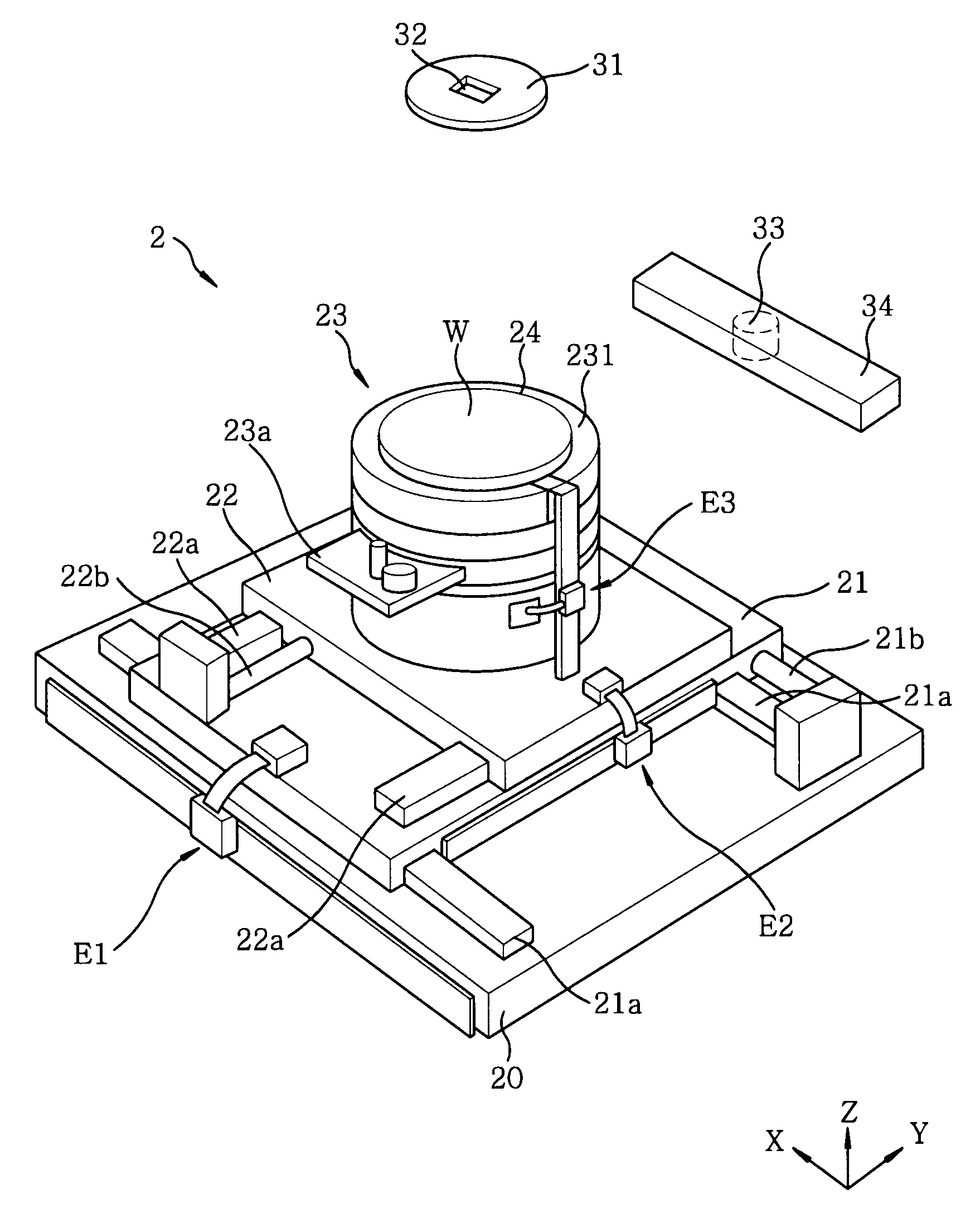
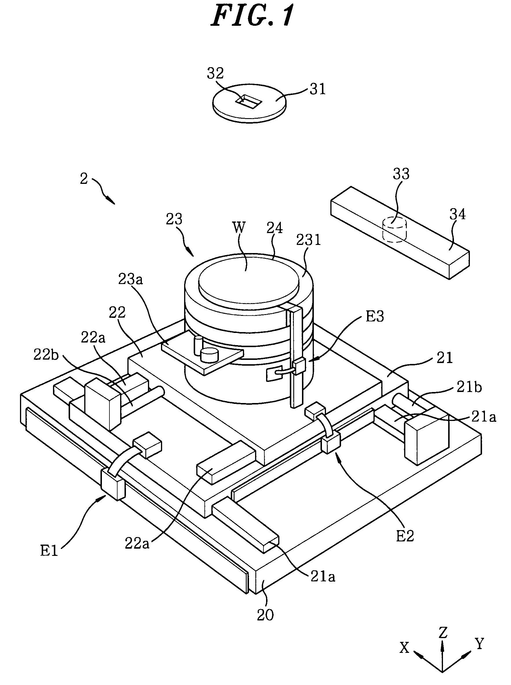
[0030]As shown in FIG. 1, a probe apparatus 1 of the present embodiment includes a base table 20. Provided on the base table 20 is a first stage 21 that is supported to be movable on two parallel first guide rails 21a extending in an X direction. The first stage 21 moves in an X direction by a driving force of a motor (not shown) connected to a first ball screw 21b that axially moves the first stage 21. Further, as the first stage 21 is provided in the above-described manner, a second stage 22 is provided on the first stage 21 and is supported to be movable on two parallel second guide rails 22a in a Y direction, and a second ball screw 22b axially moves the second stage 22. For convenience, the X and Y directions in the present embodiment indicate both sides of orthogonal coordinate axes on a plane. The X and Y directions in the present inventi...


PUM


Abstract

A probe apparatus includes a first stage, a second stage, a third stage and an image pickup. A Z position measuring unit measures a Z direction position of the mounting table and has a Z scale extending in the Z direction and a reading unit for reading the Z scale. A computation unit obtains a calculated contact position between the probes and the electrode pads of the substrate to be inspected based on images picked up by the image pickup with respect to a coordinate position on coordinates of a driving system which includes a Z direction position and X and Y direction positions measured by a measuring unit for measuring X and Y direction positions of the mounting table. A correcting unit corrects the Z direction position of the contact position based on the change amount thereof for a next contact operation.

Description

FIELD OF THE INVENTION[0001]The present invention relates to a technical field of a probe apparatus for sequentially measuring electrical characteristics of chips to be inspected by bringing probes of a probe card into contact with electrode pads of the chips to be inspected by moving a mounting table which mounts thereon a substrate to be inspected on which the chips to be inspected are arranged.BACKGROUND OF THE INVENTION[0002]Conventionally, in order to test electrical characteristics of IC chips formed on a semiconductor wafer, a probe test is performed on the wafer by using a probe apparatus. The probe apparatus includes a wafer stage capable of moving in X, Y and Z directions and rotating about a Z axis and is configured to test the electrical characteristics of the IC chips by brining probes, e.g., probe needles, of a probe card provided above the wafer stage into contact with electrode pads of the IC chips of the wafer, and controls a position of the wafer stage so that the ...

Claims


Application Information

Patent Timeline
Patent Type & Authority Applications(United States)
IPC IPC(8): G01R31/02G01R31/28G01P21/00
CPCG01R31/2891G01R31/2887H01L22/00G01R1/073
Inventor YANO, KAZUYASHIMOYAMA, HIROSHISUZUKI, MASARU
Owner TOKYO ELECTRON LTD
Why Eureka
Try Eureka