Output buffer device

Active Publication Date: 2009-08-06
MACRONIX INT CO LTD
View PDF6 Cites 11 Cited by
  • Summary
  • Abstract
  • Description
  • Claims
  • Application Information

AI Technical Summary

Benefits of technology

[0008]An objective of the present invention is to provide an output buffer with minimizing short-circuit current existing between PMOS transistor and NMOS transistor when they are switched simultaneously

Problems solved by technology

In particular, the need for fast processing of data and interface speed is becoming important, however, some noise issues exist for output buffer design such as simultaneous switching noise (SSN).
The well-known issue, SSN, is a phenomenon associated with transistors switching where the gate voltage can appear to be less than the local ground potential, causing the unstable operation of a logic gate.
As far as the output buffer techniq

Method used


Image

  • Output buffer device
  • Output buffer device
  • Output buffer device

Examples


first embodiment

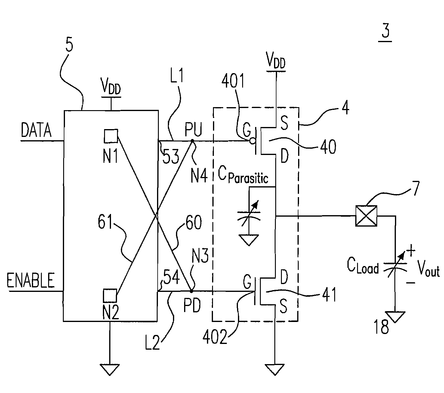
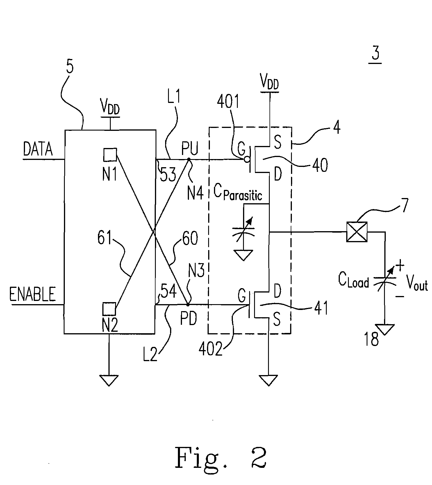
[0023]FIG. 2 shows a circuit of an output buffer according to a first embodiment of the invention, and the output buffer 3 includes an output stage 4 formed by a first switch 40 having a first control terminal 401 and a second switch 41 having a second control terminal 402, which are electrically connected in series between a supply line at a supply potential VDD and a ground line at a ground potential VGND. In fact, as is known, the first switch 40 is a PMOS transistor and the second switch 41 is an NMOS transistor, and a pre-driver 5, having a first output terminal L1 and a second output terminal L2 coupled to each gate terminal 401, 402 of the PMOS transistor 40 and the NMOS transistor 41, for respectively controlling each gate terminal 401, 402 of the PMOS transistor 40 and the NMOS transistor 41 in order to bring these transistors 40, and 41 to the turning-on threshold.

[0024]Next, in the detailed description from the accompanying FIG. 2, the output buffer 3 comprises a first wi...

second embodiment

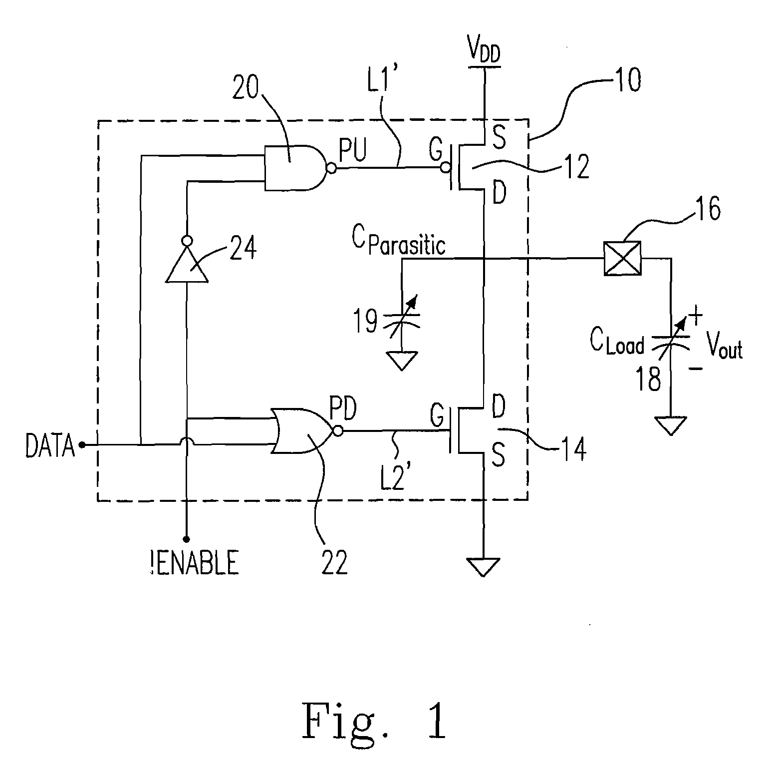
[0048]The second embodiment shows that NAND / NOR gate in the pre-driver are buffered with inverter chain. Therefore, in FIG. 6, the pre-driver 5 further provides a first inverter 71, a second inverter-like gate 72, a third inverter 73 and a fourth inverter-like gate 74 to support a high driving capacity to an NAND gate 75 and an NOR gate 76 with large loading. Here, the pre-driver 5 comprises NAND gate and the NOR gates' VGND / VDD node coupled to VGND / VDD, however, the term second inverter-like gate 72 and fourth inverter-like gate 74 differ from typical inverters owing to their VGND / VDD node being not always coupled to VGND / VDD. Still, it is required to explain that the operation characteristics of second inverter-like gate 72 and fourth inverter-like gate 74 are identical to that of typical inverters.

[0049]Referring to FIG. 6, the first inverter 71 inverts the output of the NAND gate 75, and the second inverter-like gate 72 includes a P-channel FET and a N-channel FET. The P-channel...


PUM


Abstract

A controlling output buffer slew rate method and an output buffer circuit for a memory device is provided. The output buffer include an output stage formed by a PMOS transistor and a NMOS transistor electrically connected in series, a pre-driver for respectively controlling each gate terminal of the PMOS transistor and the NMOS transistor in order to bring these transistors to the turning-on threshold, a first wire, for transmitting a pull-up signal, coupled between the output stage and the pre-driver, and a second wire, for transmitting a pull-down signal, coupled between the output stage and the pre-driver. After a DATA signal transition (logic state is changed from “H” to “L” or “L” from to “H”), the PMOS or NMOS transistor is turned off first, and then the NMOS or PMOS transistor is turned on due to the time difference between the pull-up signal and the pull-down signal.

Description

FIELD OF THE INVENTION[0001]The present invention relates to a simple output buffer. More particularly, the present invention relates to an output buffer with controlled slew rate used in integrated circuit (IC) device.BACKGROUND OF THE INVENTION[0002]Output buffer or driver circuits are employed in integrated circuit devices (such as memory devices) as a means of transferring and amplify signals, provided to the input of another device, within a device. FIG. 1 shows a conventional output buffer 10, including a pull-up PMOS transistor 12 and a pull-down NMOS transistor 14. The PMOS transistor 12 has a source terminal S coupled to a supply voltage VDD and a drain terminal D coupled to both the output pad 16 and the drain terminal D of the NMOS transistor 14. The source terminal S of the NMOS transistor 14 is coupled to a ground potential GND. The output pad 16 is typically coupled to the inputs of one or more CMOS devices. These devices are modeled as a variable load capacitor 18 and...

Claims


Application Information

Patent Timeline
IPC IPC(8): H03K19/0175
CPCG11C7/02G11C7/04G11C7/1051H03K19/00384H03K19/0013H03K19/00361G11C7/1057
Inventor LIN, YUNG FENG
Owner MACRONIX INT CO LTD
Why Eureka
Try Eureka