Asymmetrical layout for complementary metal-oxide-semiconductor integrated circuit to reduce power consumption

Inactive Publication Date: 2009-03-19
KIM JOYCE
View PDF4 Cites 2 Cited by
  • Summary
  • Abstract
  • Description
  • Claims
  • Application Information

AI Technical Summary

Benefits of technology

[0025]The various embodiments of the asymmetrical CMOS integrated circuit design layout and method for layout in accordance with the present invention provide many advantages over conventional CMOS design layouts and layout techniques, which make the asymmetrical CMOS integrated circuit design layout and method for layout in accordance with the embodiments of the present invention more useful to semiconductor manufacturers. For example, various embodiments of the asymmetrical CMOS integrated circuit design layout and method for layout in accordance with the present invention reduce power consumption by minimizing short circuit current. One embodiment of the present invention incorporates an asymmetrical polysilicon gate and diffusion, whose operation exhibits reduced current flow during operation to thereby decrease power consumption. That is, the various embodiments of the present invention provide a low-power design layout using an asymmetrical polysilicon gate and diffusion in a CMOS integrated circuit design to thereby minimize a short circuit condition, thus saving on associated unwanted power consumption. Accordingly, the various embodiments of the present invention provide a design layout and methodology that produce CMOS integrated circuits which have enhanced efficiency.

Problems solved by technology

Improving the design to decrease power consumption is a critical problem in the semiconductor manufacturing industry and has a direct correlation to the amount of heat that is generated during operation.
Reduced power consumption results in lower generation of heat.
Additionally, lower power consumption yields longer battery life in circumstances when the integrated circuit is incorporated into a battery-operated system or operated in a battery-powered mode.
Significant power is only drawn when their transistors are switching between on and off states; consequently, CMOS devices do not produce as much heat as other forms of logic such as transistor-transistor-logic (TTL).
In addition, the simplicity and comparatively low power dissipation of CMOS circuits have allowed integration densities not possible on the basis of bipolar junction transistors.
This means that the gate can be put on early in the process and then used directly as an implant mask producing a self-aligned gate (gates that are not self-aligned require overlap which increases device size and stray capacitance).
However, to speed up the designs, manufacturers have switched to gate materials which lead to lower voltage thresholds, and a modern NMOS transistor with a Vth of 200 mV has a significant subthreshold leakage current.
As a result, these devices dissipate considerable power even when not switching.
A different form of power consumption has become more prevalent as wires on chip have become narrower and the long wires have become more resistive.
Nevertheless, unwanted power consumption persists.
In summary, CMOS circuits exhibit power losses during operation.

Method used


Image

  • Asymmetrical layout for complementary metal-oxide-semiconductor integrated circuit to reduce power consumption
  • Asymmetrical layout for complementary metal-oxide-semiconductor integrated circuit to reduce power consumption
  • Asymmetrical layout for complementary metal-oxide-semiconductor integrated circuit to reduce power consumption

Examples


Embodiment Construction

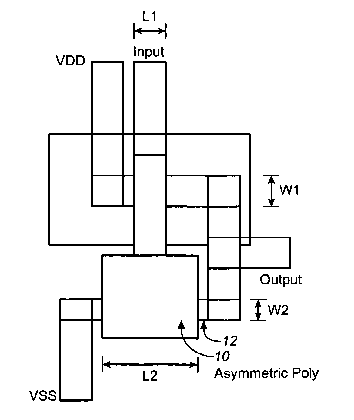
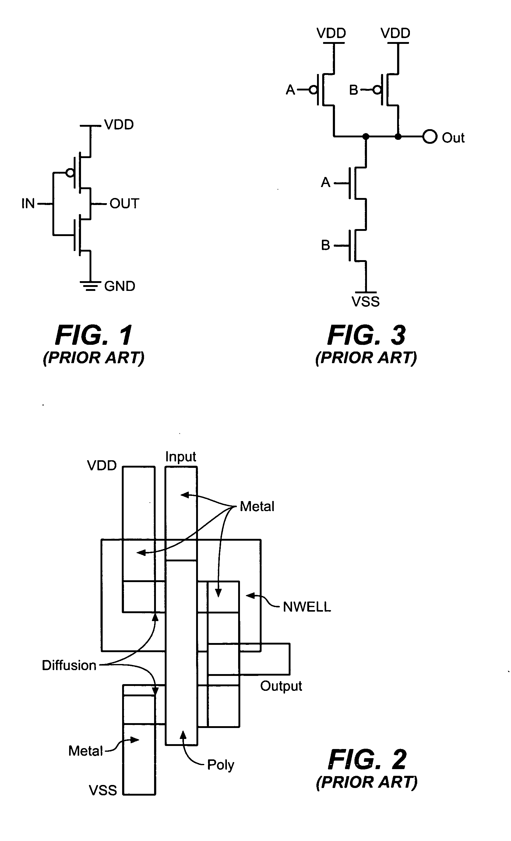
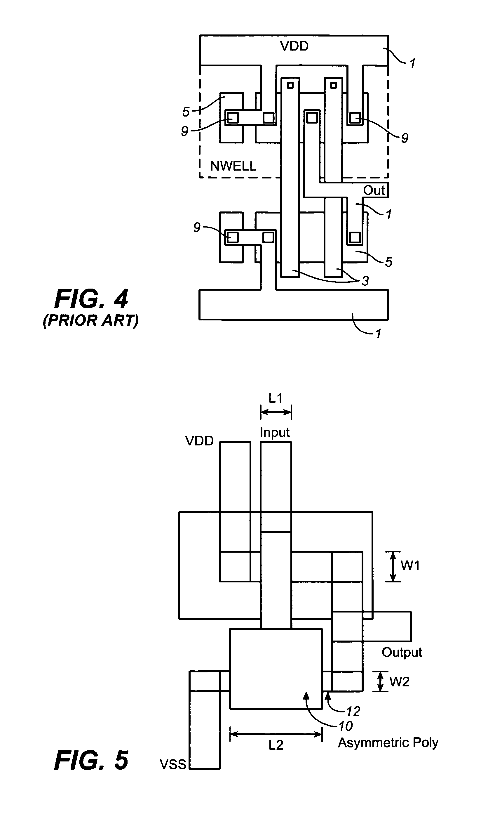
[0038]The present invention is particularly applicable to a design layout for producing a CMOS integrated circuit, and it is in this context that the various embodiments of the present invention will be described. It will be appreciated that while the asymmetrical CMOS integrated circuit design layout and method for layout in accordance with the one embodiment of the present invention will be described for an inverter circuit, the asymmetrical CMOS integrated circuit design layout and method for layout have greater utility, since they may be employed for producing other CMOS integrated circuits not described in detail herein. The underlying principle of various embodiments of the present invention is to provide an asymmetrical polysilicon gate and diffusion in the CMOS integrated circuit design layout.

[0039]FIG. 5 illustrates an example of an asymmetrical CMOS integrated circuit design layout for an inverter circuit in accordance with one embodiment of the present invention. The asy...


PUM


Abstract

A Complementary Metal-Oxide-Semiconductor (CMOS) integrated circuit design layout incorporating an asymmetrical polysilicon gate and diffusion is disclosed. The resulting asymmetrical CMOS integrated circuit exhibits reduced current flow during operation to thereby decrease power consumption.

Description

BACKGROUND OF THE INVENTION[0001]1. Field of the Invention[0002]The present invention relates generally to the design of integrated circuits for fabrication by a semiconductor manufacturing process and, more particularly, to an asymmetrical layout for an integrated circuit having reduced power consumption during operation. Specifically, one embodiment of the present invention provides a layout for a Complementary Metal-Oxide-Semiconductor (CMOS) integrated circuit design incorporating an asymmetrical polysilicon gate and diffusion, which exhibits reduced current flow during operation to thereby decrease power consumption, and a method for layout.[0003]2. Description of the Prior Art[0004]The semiconductor manufacturing industry is continually evolving semiconductor device designs and fabrication processes and developing new processes to produce smaller and smaller geometries of the designs being manufactured, because smaller semiconductor devices typically consume less power, genera...

Claims


Application Information

Patent Timeline
IPC IPC(8): H01L27/092G06F17/50
CPCH01L27/0207
Inventor KIM, JOYCE
Owner KIM JOYCE
Why Eureka
Try Eureka