Novel self-aligned etch method for patterning small critical dimensions

a self-aligning, critical dimension technology, applied in the field of self-aligning etching, can solve the problems of undesirable etching damage to the top side and corners of the layer or layers underlying the polymer layer, the difficulty of common photolithographic patterning of small geometries, and the inability to produce desired small geometries. to achieve the effect of minimizing or preventing damage to the upper surface and corners of raised device features

Inactive Publication Date: 2009-08-13
TAIWAN SEMICON MFG CO LTD
View PDF7 Cites 13 Cited by
  • Summary
  • Abstract
  • Description
  • Claims
  • Application Information

AI Technical Summary

Benefits of technology

[0005]To solve the aforementioned problem, an etching process is disclosed for a self-aligned etch technique that enables the formation of small critical dimension features in semiconductor devices, while minimizing or preventing damage to upper surfaces and corners of raised device features.

Problems solved by technology

Common photolithographic patterning of small geometries, however, is increasingly difficult, especially in trench structures, to the point that photolithographic masking techniques may no longer be efficient or even capable of producing desired small geometries (e.g., less than 10 nanometers (nm)).
The problem with this technique is that it can result in undesirable etching damage to the top side and corners of the layer or layers underlying the polymer layer during subsequent etching steps. FIG. 1 illustrates typical etching results that can occur, which include etching off the top surface 2 and rounding of the corners 4, 6 of the layer to be etched 8.
This problem becomes more acute as trench sizes shrink

Method used


Image

  • Novel self-aligned etch method for patterning small critical dimensions
  • Novel self-aligned etch method for patterning small critical dimensions
  • Novel self-aligned etch method for patterning small critical dimensions

Examples


Embodiment Construction

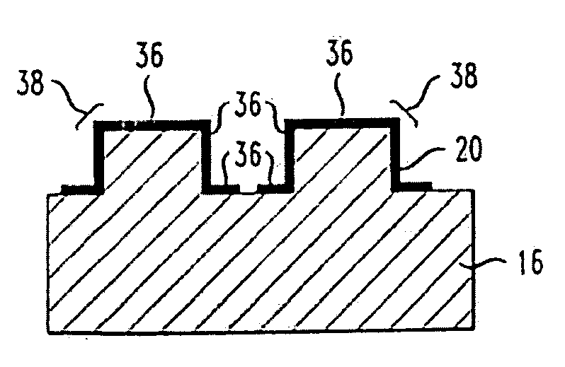
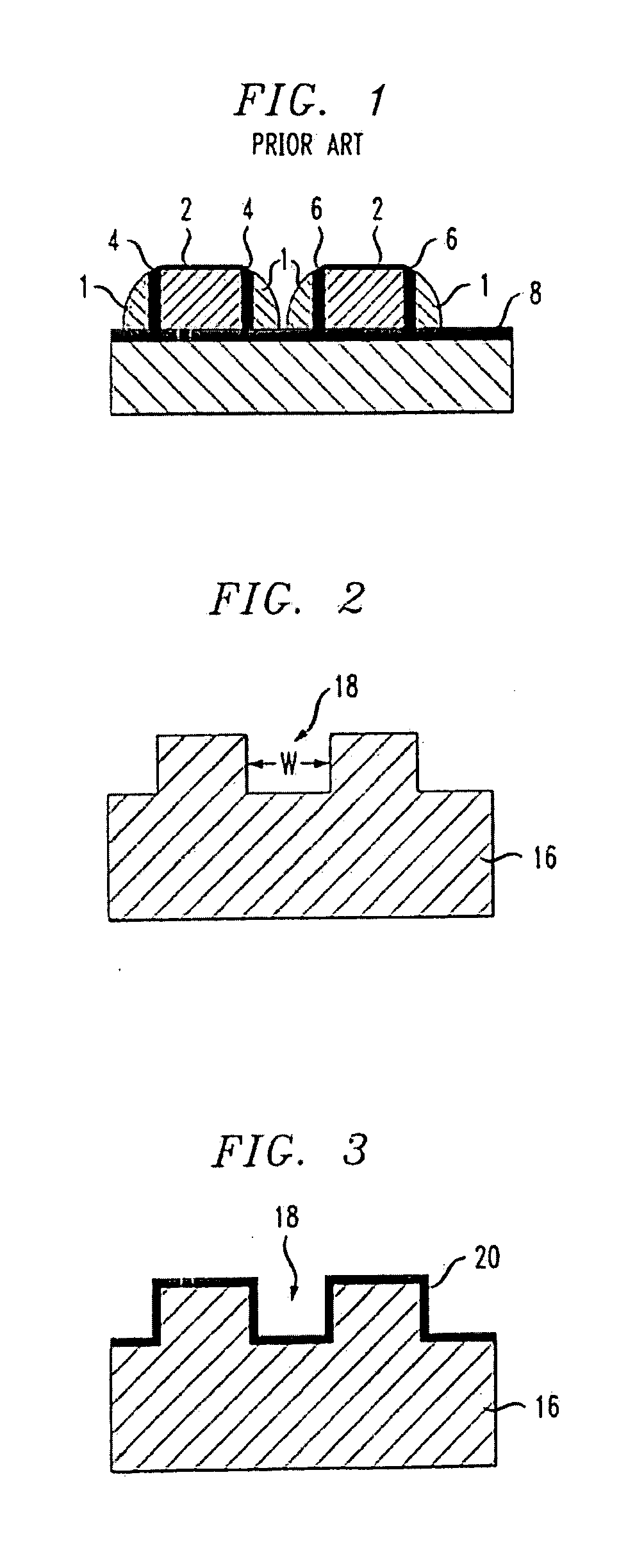
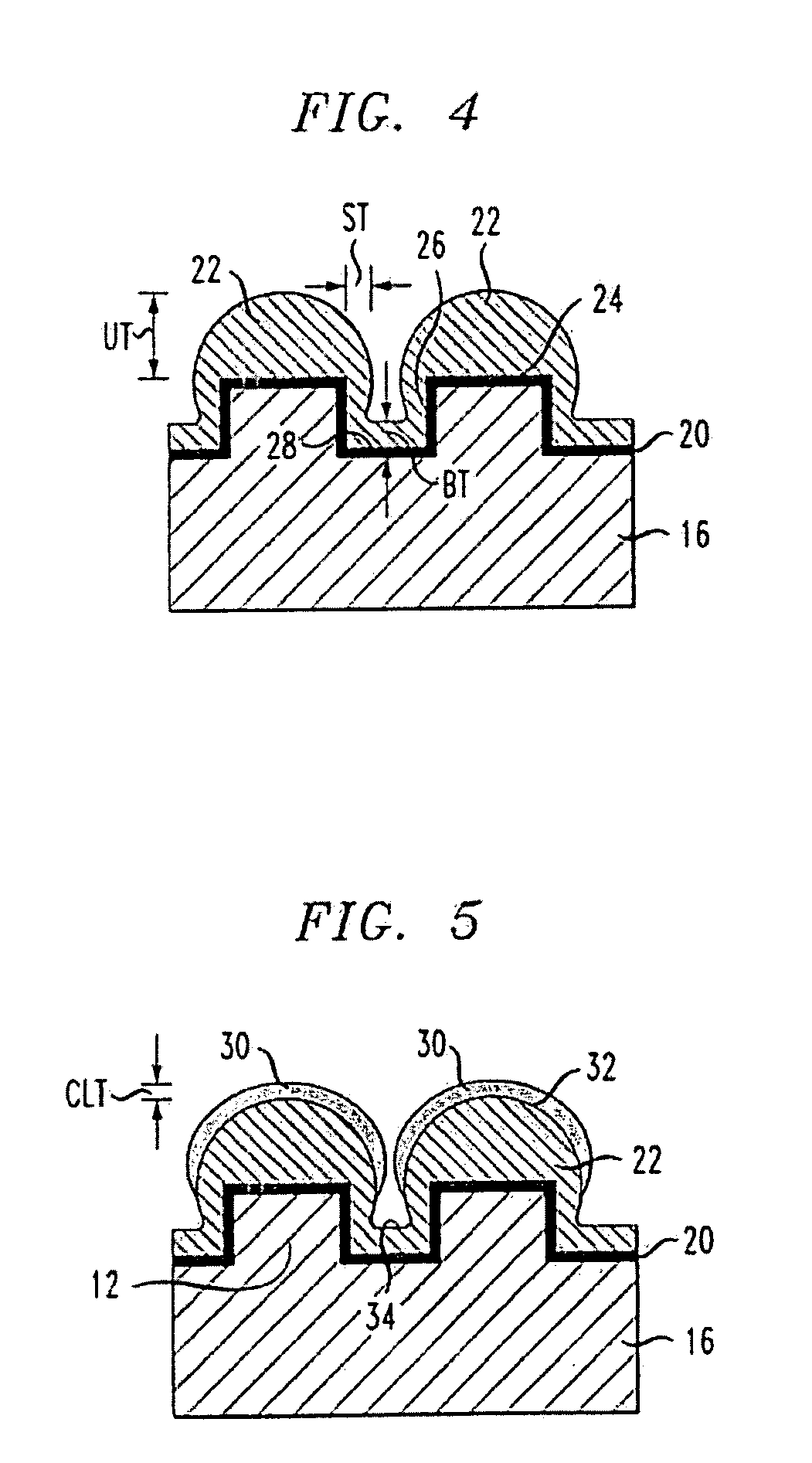
[0019]According to an embodiment of the present invention, disclosed herein is a method for etching through an etched film overlaying a repeating trench of a base structure without photolithography and without causing damage to layers adjacent to the trenches. A CF polymer is deposited on the exposed surfaces of a baseline structure, thus achieving a high aspect ratio (>4) trench (e.g., one in which the depth of the trench is more than four times its width). A cap layer of SiOCl polymer is deposited over the CF polymer using SiCl4, HBr and O2. After depositing CF polymer, the aspect ratio of the polymer trench feature become higher. The higher aspect ratio of the CF polymer trench allows only a very thin layer of SiOCl polymer to be deposited at the bottom of the polymer trench. A comparatively thicker layer of SiOCl will be deposited on the top portions of the device features. Because the SiOCl polymer has good selectivity to O2 based etching, the polymer layer deposited on the top...


PUM

PropertyMeasurementUnit
widthaaaaaaaaaa
aspect ratioaaaaaaaaaa
thicknessaaaaaaaaaa

Abstract

A method is disclosed for etching an integrated circuit structure within a trench. A layer to be etched is applied over the structure and within the trench. A CF-based polymer is deposited over the layer to be etched followed by deposition of a capping layer of SiOCl-based polymer. The CF-based polymer reduces the width of the trench to such an extent that little or no SiOCl-based polymer is deposited at the bottom of the trench. An O2 plasma etch is performed to etch through the CF-based polymer at the bottom of the trench. The O2 plasma etch has little effect on the SiOCl-based polymer, the thus the upper surfaces of the structure remain covered with polymer. Thus, these upper surfaces remain fully protected during subsequent etching of the layer to be etched.

Description

FIELD OF THE INVENTION[0001]The disclosure relates generally to an etch technique for efficiently creating small critical dimension patterns during fabrication of semiconductor devices, and more particularly to a self-aligned etch technique that enables etching through a single thin film or composite film in small critical dimensional trench structures.BACKGROUND OF THE INVENTION[0002]As device sizes continue to shrink, the critical dimensions of photolithographic features also must shrink. Common photolithographic patterning of small geometries, however, is increasingly difficult, especially in trench structures, to the point that photolithographic masking techniques may no longer be efficient or even capable of producing desired small geometries (e.g., less than 10 nanometers (nm)). A variety of techniques have been suggested, such as reflowing the patterned photoresist mask, or using light having a carefully selected wavelength, to create a desirably small pattern on the mask.[00...

Claims


Application Information

Patent Timeline
Patent Type & Authority Applications(United States)
IPC IPC(8): H01L21/302
CPCH01L21/0337H01L21/32139H01L21/31144H01L21/0338
Inventor LEE, CHUN-HUNGCHUNG, CHIA-CHICHEN, HSIN-CHIHXU, JEFF J.CHEN, NENG-KUO
Owner TAIWAN SEMICON MFG CO LTD
Why Eureka
Try Eureka