Voltage regulator
- Summary
- Abstract
- Description
- Claims
- Application Information
AI Technical Summary
Benefits of technology
Problems solved by technology
Method used
Image
Examples
first embodiment
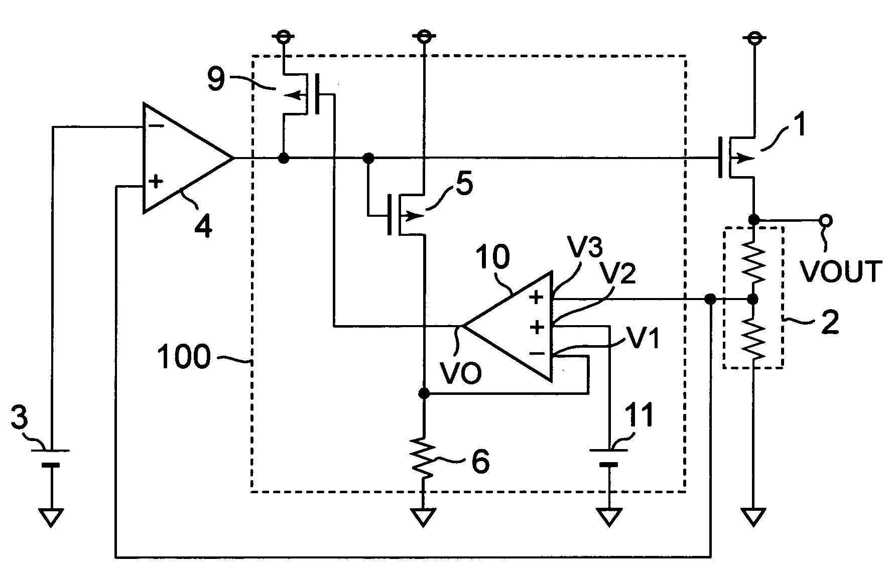
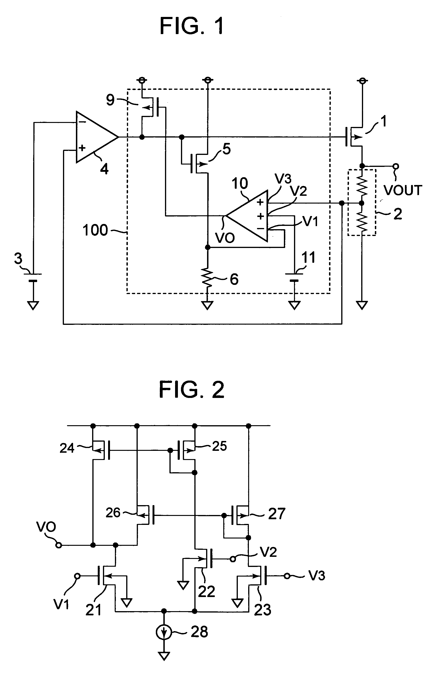
[0027]FIG. 1 is a circuit diagram of a voltage regulator according to the present invention.
[0028]The voltage regulator according to the first embodiment includes an output transistor 1 which is a PMOS transistor, an output voltage divider circuit 2, a reference voltage circuit 3, an error amplifier 4, and an overcurrent protection circuit 100. The overcurrent protection circuit 100 includes an output current detection transistor 5 which is a PMOS transistor, a detection resistor 6, an output current control transistor 9 which is a PMOS transistor, a second error amplifier 10, and a second reference voltage circuit 11.
[0029]The output voltage divider circuit 2 has an input terminal connected to an output terminal Vout and an output terminal connected to a non-inverting input terminal of the error amplifier 4. The reference voltage circuit 3 has an output terminal connected to an inverting input terminal of the error amplifier 4. The error amplifier 4 has an output terminal connected...
second embodiment
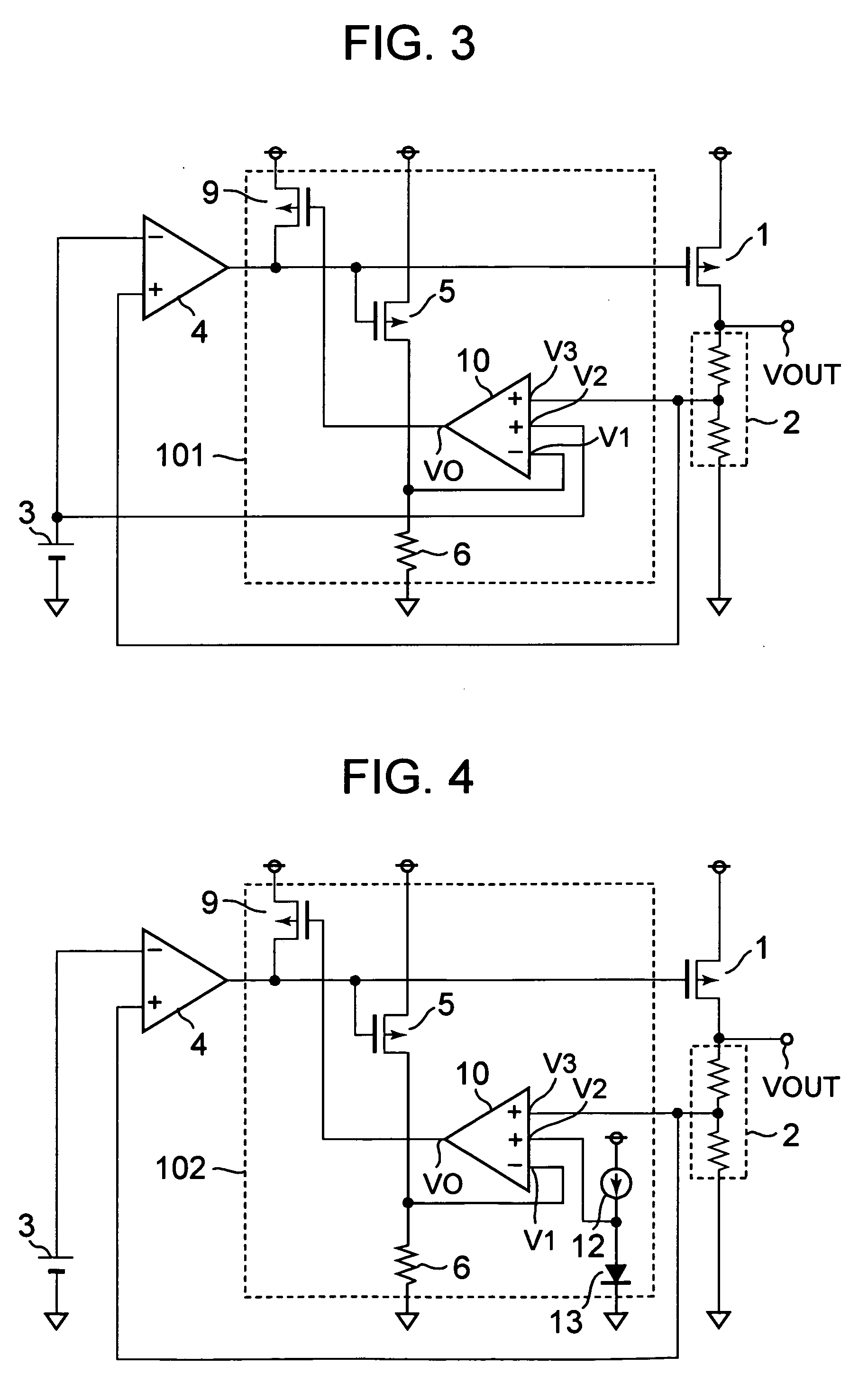
[0036]The second error amplifier 10 of FIG. 2 described above is applicable to a voltage regulator according to the present invention, which is illustrated in FIG. 3 and FIG. 4.
[0037]The overcurrent protection circuit 100 as described above has a function of operating as follows to protect the circuit from the overcurrent.
[0038]In the case where the output current of the output terminal Vout increases, the detection current in accordance with the output current flows through the output current detection transistor 5. When the detection current flows through the detection resistor 6, the voltage of the inverting input terminal V1 of the second error amplifier 10 increases. The second reference voltage Vref2 is input to the first non-inverting input terminal V2 of the second error amplifier 10, and the divided voltage Vdiv is input to the second non-inverting input terminal V3 thereof. In a normal operating state, the divided voltage Vdiv is equal to the second reference voltage Vref2...
PUM
 Abstract
Description
Claims
Application Information


