Check patentability & draft patents in minutes with Patsnap Eureka AI!

Debug device for embedded systems and method thereof

Inactive Publication Date: 2009-08-27
UNIVERSAL SCIENTIFIC INDUSTRIAL (SHANGHAI) CO LTD +1
View PDF9 Cites 11 Cited by
  • Summary
  • Abstract
  • Description
  • Claims
  • Application Information

AI Technical Summary

Benefits of technology

[0012]Thus, in accordance with the above-mentioned implementation method, the present invention can, by means of a debug device, read the data transmitted through a data bus on the data flash interface of the embedde

Problems solved by technology

However, for embedded systems, there is no BIOS installed inside, which is different from computer systems.
Hence, when debugging an embedded system a method as described above for computer systems cannot be used.
Besides, the processors used in embedded systems may differ from those in computer systems since processor vendors adopt various interfaces, and thus the entire development of embedded systems could be inevitably full of difficulties and challenges.
Although the embedded system implemented by means of the present Marvell PXA320 processor can perform single-step debug through RS-232 transmission, this approach simply displays the instructions currently executed by the embedded system onto a display interface, whereas in terms of debugging, it is impossible to pinpoint the location of hardware failure in the embedded system through the displayed instructions.

Method used


Image

  • Debug device for embedded systems and method thereof
  • Debug device for embedded systems and method thereof
  • Debug device for embedded systems and method thereof

Examples


Embodiment Construction

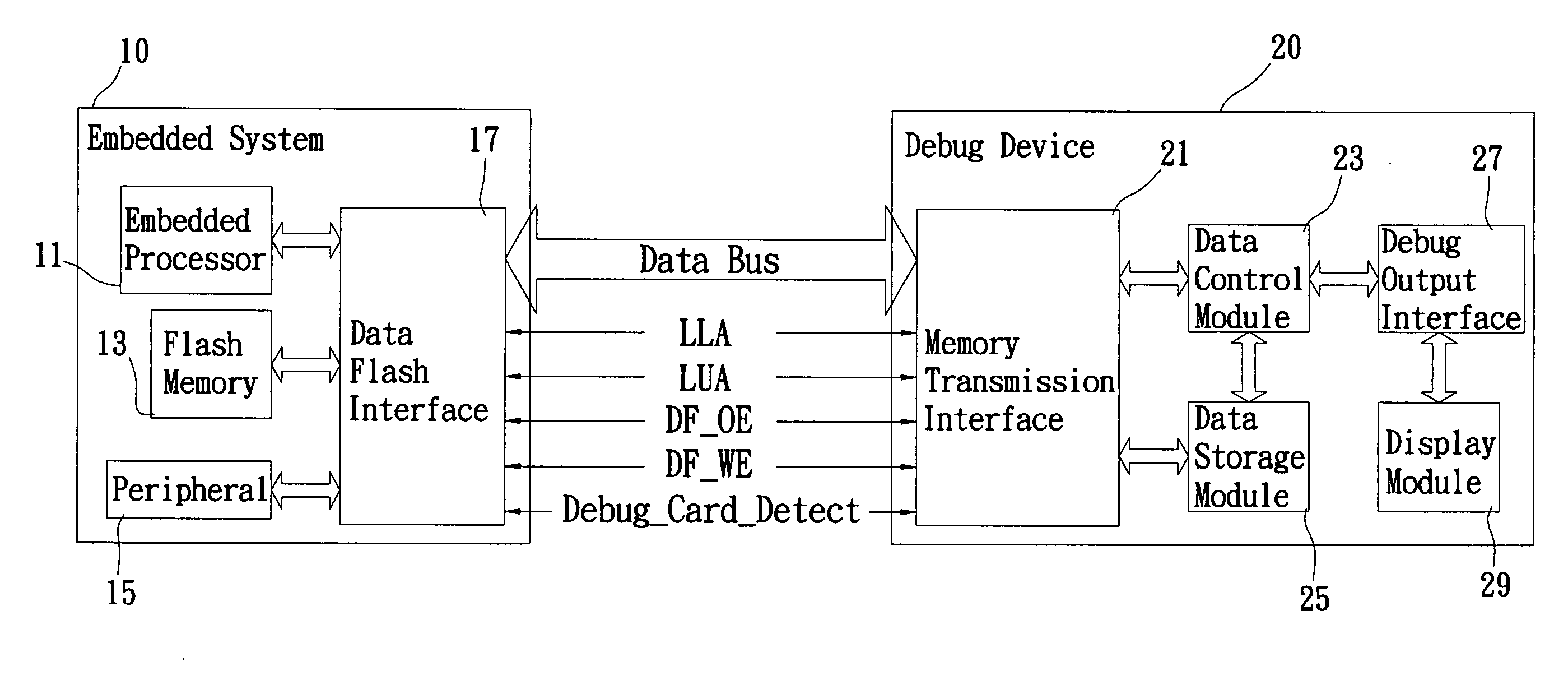
[0018]The present invention provides a debug device for performing debug on an embedded system, such that during development of the embedded system, it is possible by means of debugging, to know the data, addresses, hardware status and other relevant results occurring during booting of the embedded system, and to use the obtained information for solving the problems encountered during hardware development. The present invention reads by means of the debug device the process results from the internal boot execution of the embedded system, and by means of outputting and displaying such process results, enables debug technicians to perform debugging.

[0019]Referring to FIG. 1, the shown embodiment illustrates a function block diagram of the debug device in accordance with the present invention. The debug device 20 shown in the embodiment is coupled to an embedded system 10, and in order to enable the debug device 20 to successfully read the relevant execution results about the booting o...


PUM


Abstract

A debug device of embedded systems is provided. The embedded system includes an embedded processor for reading a bootloader from a flash memory through a data flash interface. The debug device includes a memory transmission interface, a dada storage module, a data control module and a display module. The memory transmission interface is configured to couple the data flash interface for receiving data to the data storage module. The data control module determines whether the data stored in the data storage module is data from a data bus or from the data flash interface according to whether a data control signal of the data flash interface has been triggered. The display module displays the data of the data storage module.

Description

BACKGROUND OF THE INVENTION[0001]1. Field of the Invention[0002]The present invention relates to a debug device, in particular, to a debug device for embedded systems and a method thereof.[0003]2. Description of Related Art[0004]Inside a computer system is installed a Basic Input / Output System (BIOS), which is responsible for performing the Power-On Self-Test (POST) procedure to the computer system. It is possible to assign a code to this procedure at each test point, so as to output to a specific input / output (I / O) port (e.g. I / O port 80), and such codes represent respectively a corresponding failure reason.[0005]Hence, the current method for debugging the BIOS of a computer system is to link to the Peripheral Component Interconnect (PCI) or Industry Standard Architecture (ISA) interface on a computer motherboard through a debug card, in which such a debug card provides the display circuit, and when the BIOS performs the POST procedure and a hardware error occurs, the debug card ca...

Claims


Application Information

Patent Timeline
IPC IPC(8): G06F11/32
CPCG06F11/27
Inventor HSU, PO-CHUN
Owner UNIVERSAL SCIENTIFIC INDUSTRIAL (SHANGHAI) CO LTD
Features
  • R&D
  • Intellectual Property
  • Life Sciences
  • Materials
  • Tech Scout
  • Unparalleled Data Quality
  • Higher Quality Content
  • 60% Fewer Hallucinations
Learn More