Novel combination nonvolatile integrated memory system using a universal technology most suitable for high-density, high-flexibility and high-security sim-card, smart-card and e-passport applications

a non-volatile integrated memory and universal technology, applied in static storage, digital storage, instruments, etc., can solve the problems of nand-type flash memory not fully compatible, type flash, and difficult integration on the same integrated circuit chip

Active Publication Date: 2006-06-01
CALLAHAN CELLULAR L L C
View PDF5 Cites 58 Cited by
  • Summary
  • Abstract
  • Description
  • Claims
  • Application Information

AI Technical Summary

Benefits of technology

[0031] If one of the plurality of nonvolatile memory arrays is the NAND configured flash memory, programming the selected first sub-arrays is accomplished by setting at least one bit line of the selected first sub-arrays to the second moderately high positive program voltage, at least one word line of the selected first sub-arrays to the very large positive programming voltage (+18V), at least one source line of the selected first sub-arrays to the second moderately high positive program voltage, and a bulk region of all cells of the selected first sub-array to the ground reference voltage. The first sub-arrays are programmed in approximately 200 μs.
[0032] Erasing selected second sub-arrays of the plurality of nonvolatile memory arrays configured as the NAND configured flash memory is accomplished by setting at least one word line of the selected second sub-arrays to the very large negative erasing voltage (−18V), very large negative erasing voltage (−18V), at least one source line of the selected second sub-arrays, and a bulk region of all cells of the selected second sub-array to the ground reference voltage. The second sub-arrays are erased in less than approximately 5 ms, preferably in less than approximately 2.5 ms.
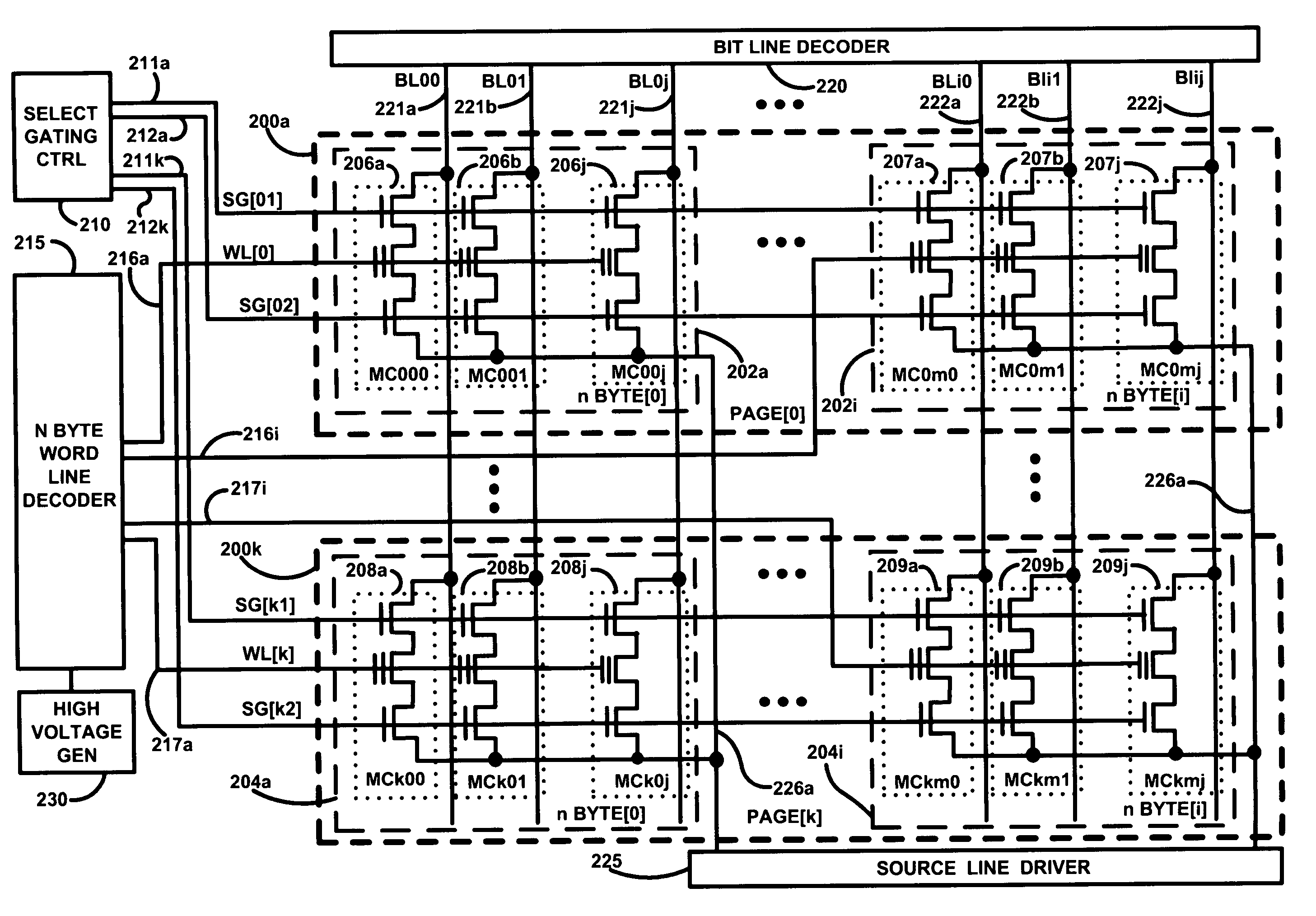
[0033] If one of the plurality of nonvolatile memory arrays is the two transistor electrically erasable programmable read only memories, programming the selected first sub-arrays is accomplished by setting at least one bit line of the selected first sub-arrays to the intermediate positive program voltage, at least one select gate line of the selected sub-arrays to the power supply voltage, at least one word line of the selected first sub-arrays to the moderately high positive program voltage, at least one source line of the selected first sub-arrays to the ground reference voltage, and a bulk region of all cells of the selected first sub-array to the ground reference voltage. Those cells of the selected sub-array not programmed but have the word line at the moderately high positive program voltage are inhibited from programming by setting select gates of non-selected cells of the selected sub-arrays to the very large positive programming voltage (+18V). Those cells of non-selected sub-arrays not programmed are inhibited from programming by setting the bit lines, word lines, source lines, and the bulk region of all cells of the non-selected first sub-array of the non-selected cells to the ground reference voltage, select gates of non-selected cells of the selected sub-arrays to the power supply voltage. The first sub-arrays are programmed in less than approximately 5 ms, preferably less than approximately 2.5 ms.
[0034] Erasing selected second sub-arrays of one of the plurality of nonvolatile memory arrays configured as the two transistor electrically erasable programmable read only memories is accomplished by setting at least one select gate line of the selected sub-arrays to the power supply voltage, at least one word line of the selected second sub-arrays to the very large negative erasing voltage (−18V), at least one bit line of the selected second sub-arrays, at least one source line of the selected second sub-arrays, and a bulk region of all cells of the selected second sub-array to the ground reference voltage. The second sub-arrays are erased in less than approximately 5 ms, preferably in less than approximately 2.5 ms.
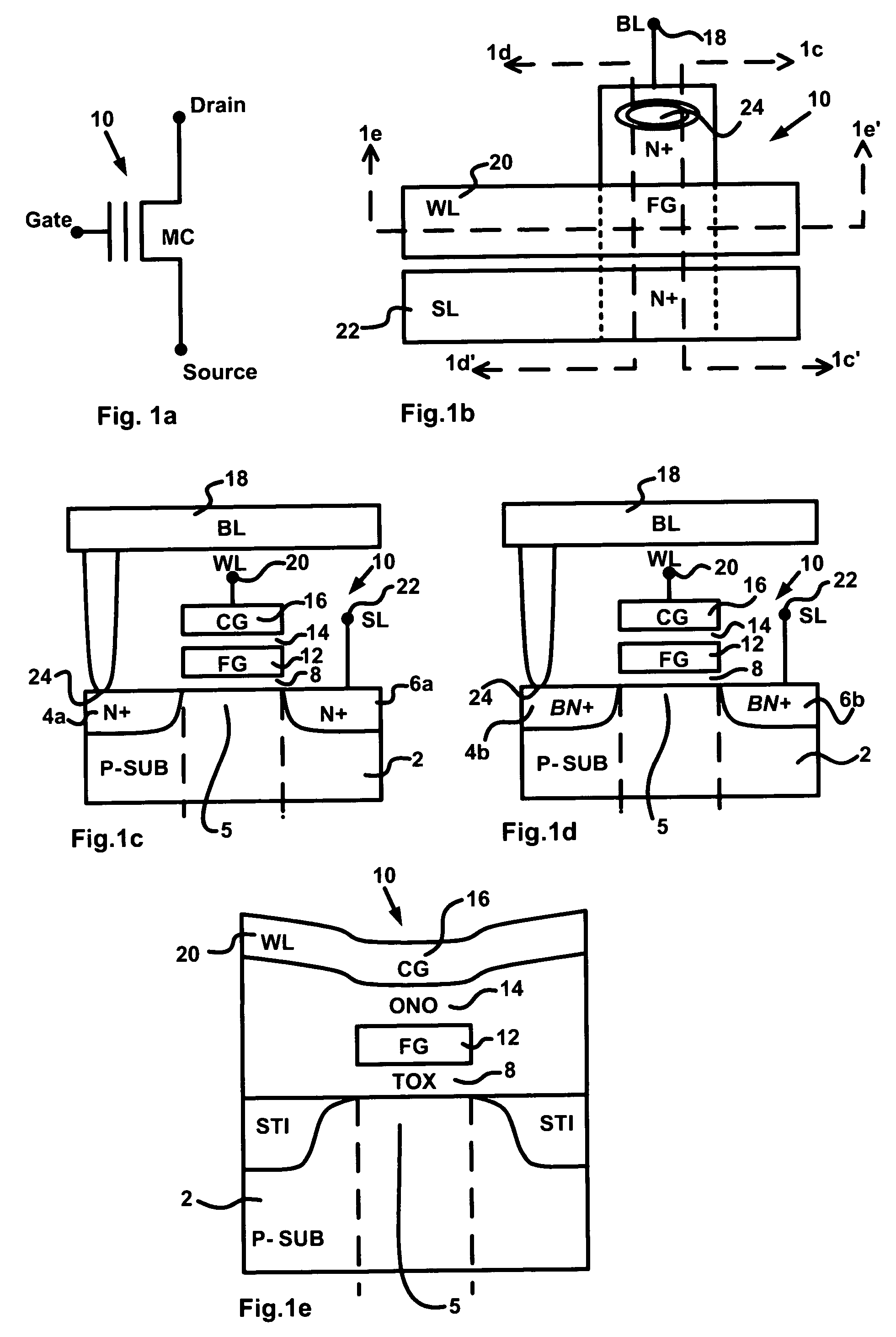
[0035] If one of the plurality of nonvolatile memory arrays is the three transistor electrically erasable programmable read only memories, programming the selected first sub-arrays is accomplished by setting at least one bit line of the selected first sub-arrays to the ground reference, at least one first select gate line of the selected sub-arrays to the power supply voltage, at least one word line of the selected first sub-arrays to the very large positive programming voltage (+18V), at least one source line of the selected first sub-arrays to the ground reference voltage, and a bulk region of all cells of the selected first sub-array to the ground reference voltage. Programming the selected first sub-arrays is further accomplished by setting at least one second select gate of the selected first sub-arrays to a ground reference voltage or to the power supply voltage. Those cells of the selected first sub-arrays not programmed but have the word line at the very large positive programming voltage (+18V) are inhibited from programming by setting bit lines of non-selected cells of the selected sub-arrays to the power supply voltage. The first sub-arrays are programmed in less than 10 μS, preferably less than approximately 1 μS.
[0036] Erasing the second selected sub-array of one of the plurality of nonvolatile memory arrays configured as the three transistor electrically erasable programmable read only memories is accomplished by setting at least one first select gate line and second select gate line of the selected sub-arrays to the power supply voltage, at least one word line of the selected second sub-arrays to the very large negative erasing voltage (−18V), at least one bit line of the selected second sub-arrays, at least one source line of the selected second sub-arrays, and a bulk region of all cells of the selected second sub-array to the ground reference voltage. The second sub-arrays are erased in less than approximately 5 ms, preferably, in less than approximately 2.5 ms.

Problems solved by technology

The three nonvolatile memory technologies (EEPROM, NOR-type and NAND-type flash memory) of prior art are process incompatible and were never intended to be manufactured on a single integrated circuit chip.
Further, the compact nature of the smart card leads to the desirability for the processor, memory function, and support functions to be placed on a single chip.
However, processes of EEPROM, NOR-type flash, NAND-type flash memories are not fully compatible in the present technology and are difficult to integrate on the same integrated circuit chip.
Obviously, using the big 1-transisitor NOR Flash and the bigger EEPROM cell to store personalized biometric data is wasteful of space.
The cells size of the EEPROM and NOR-type Flash memories no longer make these memories a cost effective solution to store personalized biometric data.
The traditional large cell size of EEPROM technology is essentially non-scalable below 0.25 μm and thus it is not suitable for storing memory density higher than 1 Mb (128 KB).
Nonvolatility requires the device to retain data without power applied for the lifetime of the application.
Both of the reliability requirements of endurance and data retention have associated failure rates, which must be minimized.

Method used


Image

  • Novel combination nonvolatile integrated memory system using a universal technology most suitable for high-density, high-flexibility and high-security sim-card, smart-card and e-passport applications
  • Novel combination nonvolatile integrated memory system using a universal technology most suitable for high-density, high-flexibility and high-security sim-card, smart-card and e-passport applications
  • Novel combination nonvolatile integrated memory system using a universal technology most suitable for high-density, high-flexibility and high-security sim-card, smart-card and e-passport applications

Examples


Embodiment Construction

[0061] The present invention is a unified process technology that permits integration of three kinds of in-system re-writable nonvolatile memories of EEPROM, NOR-type Flash nonvolatile memory and NAND-type Flash nonvolatile memory in one integrated circuit chip such as a system-on-a-chip for applications such as a smart card. The EEPROM, the NOR-type Flash nonvolatile memory, and the NAND-type nonvolatile memory are designed to be altered in system, with minimal hardware or software difficulty. The number of times the device must be altered within its application determines the endurance requirement of the device. Nonvolatility requires the device to retain data without power applied for the lifetime of the application and the lifetime of the application determines the data retention requirement of the device. Both of the reliability requirements of endurance and data retention have associated failure rates, which must be minimized. Since NOR-type flash memories are employed as the ...


PUM


Abstract

A combination EEPROM, NOR-type Flash and NAND-type Flash nonvolatile memory contains memory cells in which a floating gate transistor forms a NAND-type Flash nonvolatile memory cell, forms a NOR-type Flash nonvolatile memory cells and with one or two select transistors forms a two and three transistor EEPROM cell. The nonvolatile memory cells use a large positive programming voltage (+18V) applied to the word lines or select gating lines for programming the memory cells and a large negative erasing voltage (−18V) applied to the word lines or select gating lines for erasing the memory cells. The NOR-type Flash nonvolatile memory array is used to store code of embedded processor programs or application programs for smart cards. The EEPROM array is preferably used to store byte alterable data and NAND-type Flash nonvolatile memory array is used to store personalized biometric data such as Iris, DNA, facial picture and finger prints.

Description

[0001] This application claims priority to U.S. Provisional Patent Application No. 60 / 631,197, filed Nov. 26, 2004, and herein incorporated by reference in its entirety. RELATED PATENT APPLICATIONS [0002]“A Novel Monolithic, Combination Nonvolatile Memory Allowing Byte, Page a Cell Array Using a Unified Cell Structure and Technology with a New Scheme of Decoder and Layout”, U.S. patent application Ser. No. 10 / 223,208, filed Aug. 19, 2002, assigned to the same assignee as the present invention, and herein incorporated by reference. [0003]“A Novel Monolithic, Combination Nonvolatile Memory Allowing Byte, Page and Block Write with No Disturb and Divided-Well in the Cell Array Using a Unified Cell Structure and Technology with a New Scheme of Decoder and Layout”, U.S. patent application Ser. No. 10 / 351,180, filed Jan. 24, 2003, assigned to the same assignee as the present invention, and herein incorporated by reference. [0004]“A Combination Nonvolatile Memory Using Unified technology wi...

Claims


Application Information

Patent Timeline
Patent Type & Authority Applications(United States)
IPC IPC(8): G11C16/04
CPCG11C16/04
Inventor LEE, PETER W.
Owner CALLAHAN CELLULAR L L C
Why Eureka
Try Eureka