

Apparatus For Trapping Residual Product Of Semiconductor Manufacturing Process
- Summary
- Abstract
- Description
- Claims
- Application Information
AI Technical Summary
Benefits of technology
Problems solved by technology
Method used
Image

Examples
Embodiment Construction
[0039]Hereinafter, an exemplary embodiment of the present invention will be described in detail with reference to the accompanying drawings.
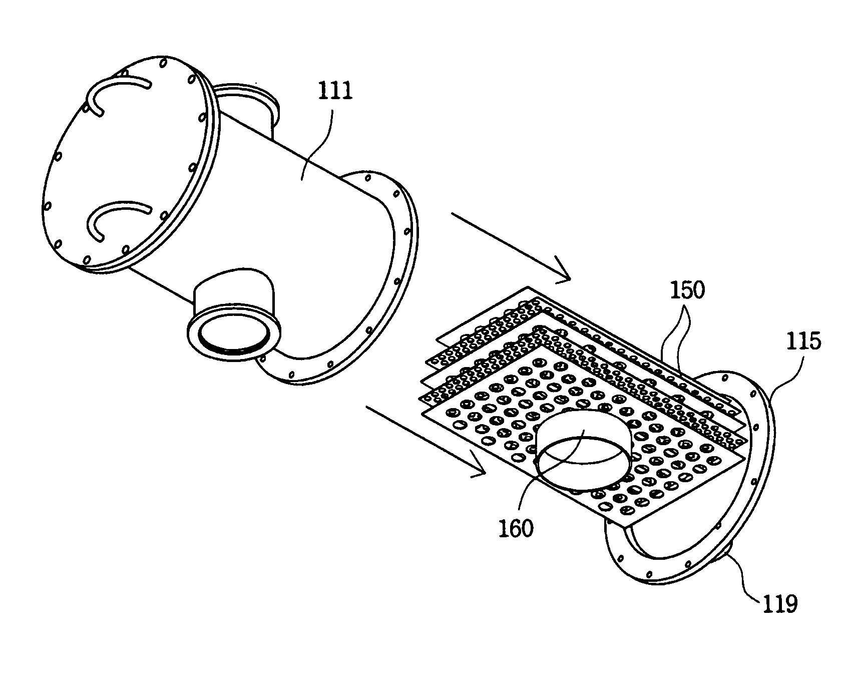
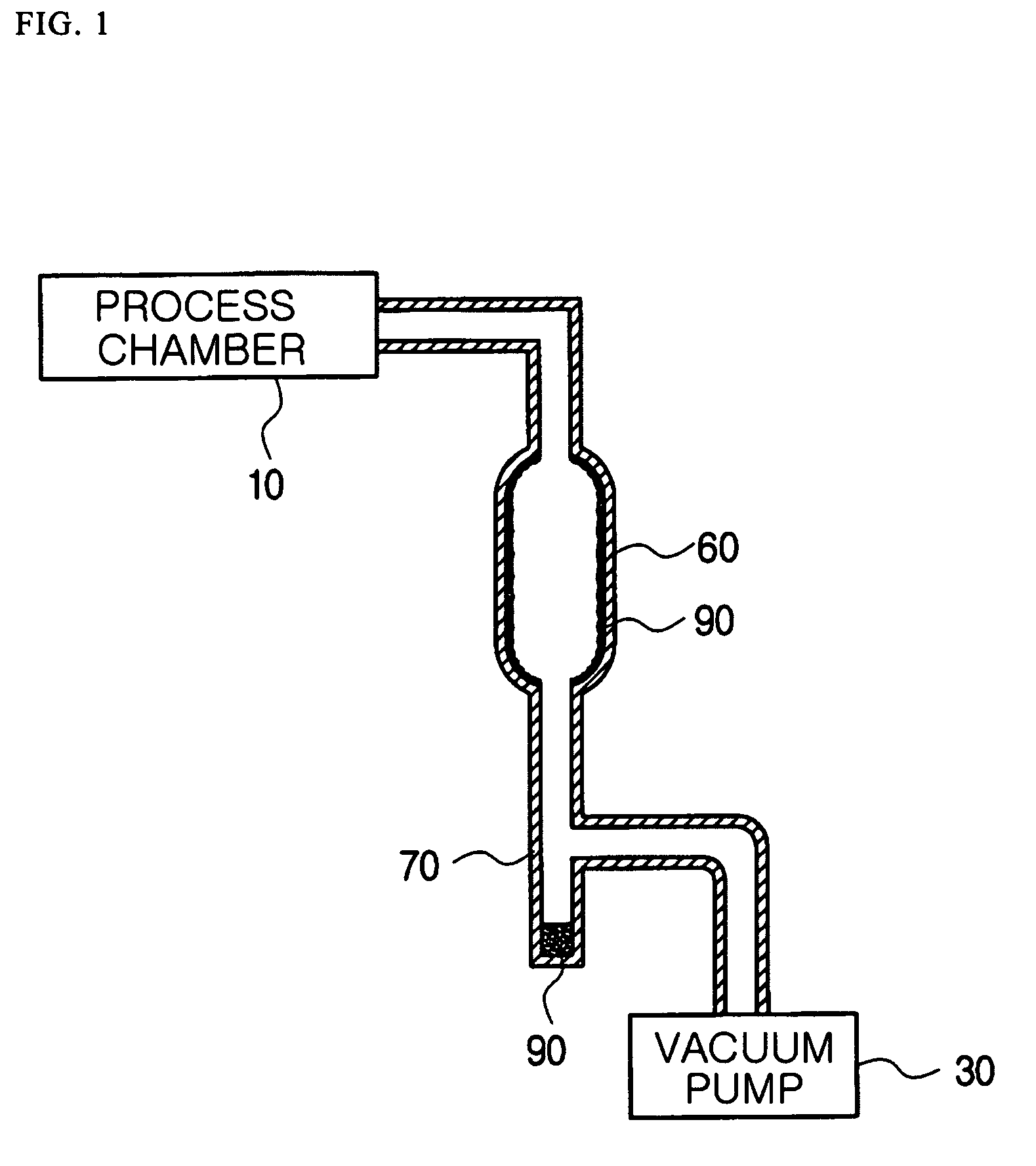
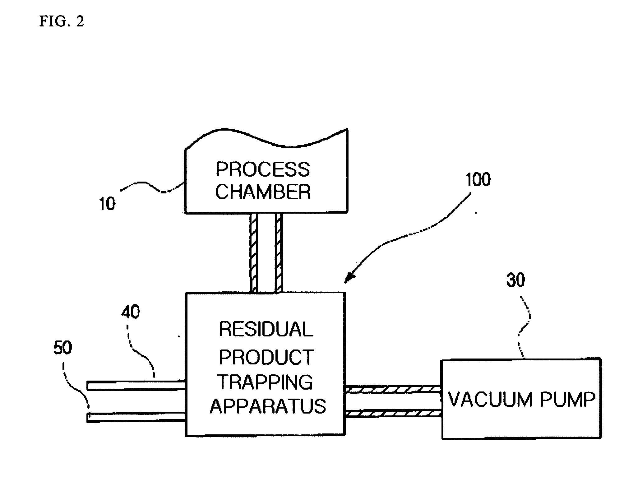
[0040]FIG. 2 shows a connection relation between a residual product trapping apparatus and a process chamber according to an embodiment of the present invention.
[0041]Referring to FIG. 2, the residual product trapping apparatus 100 is connected to a process chamber 10 in which a residual product of reaction is generated in a thin film deposition or etching process during a semiconductor / LCD manufacturing process or its equivalent process. The other side of the residual product trapping apparatus 100 is connected to a vacuum pump 30 which makes the inner side of the process chamber 10 vacuous by means of the residual product trapping apparatus 100.
[0042]Further, the residual product trapping apparatus 100 is also connected to a refrigerant supply pipe 40 and a refrigerant discharge pipe 50 which are linked to an external refrigerant tank (not sho...
PUM
| Property | Measurement | Unit |
|---|---|---|
| Temperature | aaaaa | aaaaa |
| Shape | aaaaa | aaaaa |
Abstract
Description
Claims
Application Information